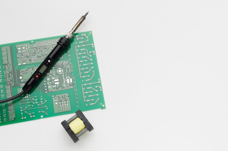
In the PCB design world, where every fraction has significance, the hole size hardly escapes a designer’s attention. The PCB drill size plays an important role in the performance of the whole product during the creativity and reliability phase Observance of drill ”s depth and maximum lead diameter is necessary for PCB designers to achieve design standards which enable them to create high-caliber boards also in to the high component densities.
Why does drill size matter?

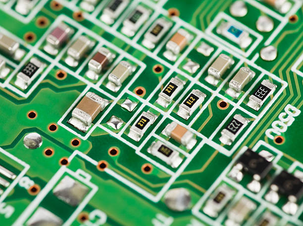
The drill size during mini-printed circuit boards (PCBs) fabrication serves as the key highlight for component layout and ultimately the optimum performance of the board. Permitting an inaccurate drill size can cause problems like misalignment of the components, low conductivity, low component density and circuit breakdown. To drill accurate holes, you need to be sure that the size of the drill is right for meeting the specific demands of the design.
PCB Drill Sizes
This table could list common drill sizes and their corresponding hole diameters:
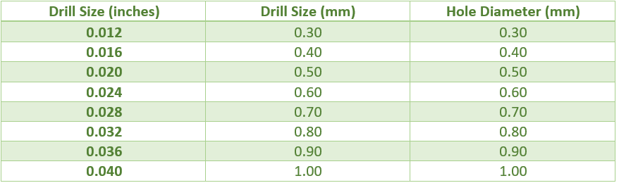
This table provides, in a nutshell, the calculation of drill size into a particular hole. Also, it is worth mentioning that the drill sizes may differ from one manufacturer to another, as well as in other aspects regarding the PCB design.
Standard PCB Drill Sizes Chart
Here you can see an example of the table that may appear on a blog about the slot sizes of a default standard sizes PCB. This table lists commonly used drill sizes in PCB manufacturing:
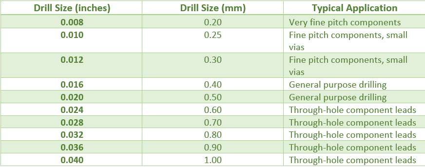
Here is the table that summarizes the common drill sizes that designers and manufacturers should use when choosing a certain drill for a PCB (printed circuit board) based on the application and the components being used. Information from the corresponding manufacturer will and should always be assessed for its suitability and their recommendations.
Chart of drill sizes that might be used on PC boards
Here’s a chart listing drill sizes commonly used on PCBs, along with their corresponding diameters in inches and millimeters:
This graph includes a range of drill sizes that are commonly used for print circuit board crafting, corresponding to each type of application as well. It should be noted that the particular drill sizes used can specifically depend on certain PCB design needs and the equipment features of the manufacturer.
Factors Influencing Drill Size Selection
However, in the future, the trend towards simplified connection sizes and increased drilling precision will continue. The drill manufacturing industry will more likely stay in the technological innovation pathway to come with new and small drills, while their accuracy ratios will increase. This tendency will allow the designers to have the privilege of creating PCBs with extra dimensions of complexity and functionality as a result of the innovation in the field.
Latest Trends and Technologies
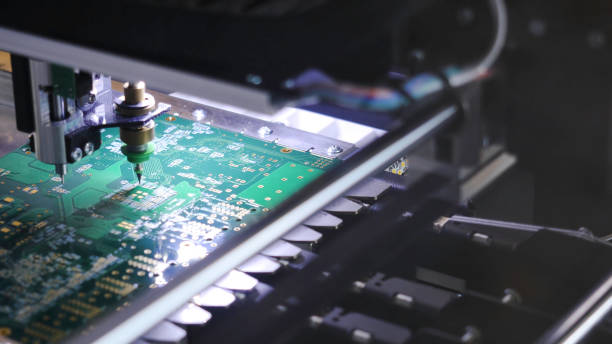
Technological advances, combined with new techniques and technologies, have brought more precision and productivity to the science of drilling. An example of a laser drill is when hole wall as small as required can be created with high precision, opening up new possibilities for PCB design and high design productivity standard.
PCB Shape and Size
The shape and size of the PCB not only determine the functionality, but above all, are important factors that determine the manufacturability and cost at the same time. In this article, we will cover the spectrum of PCB shape and size lately and the effect that can have on your PCB layout.
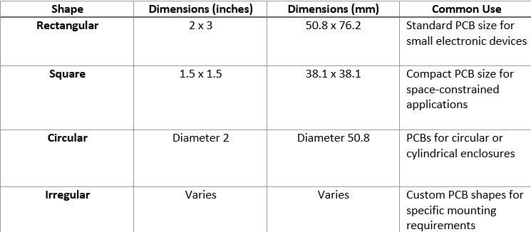
PCB Shape
Usually, the features of a printed circuit board depend on the housing or enclosure where it will be installed. Different shapes and variants of PCB are available, including rectangles, squares, circles, and irregular shapes. The choice of shape factors in on the application’s requirements and the availability of an of an area for mounting the PCB.
Nowadays, it seems that we are experiencing a microscale shape revolution in mobile devices, and non-traditional PCB shapes are highly demanded. With numerous irregular-shaped PCBs gaining traction nowadays, like boards that feature wins, notches, or curves, the designer is on a mission to save space optimally and create the most eye-catching outlay.
PCB Size
The size of a PCB is determined by the dimensions of the board, which are normally depicted via a length and a width (in inches or millimeters). A smaller PCB (printed circuit board) is the product of having fewer and smaller components, less complicated circuitry, and application-specific requirements.

The smaller sizes of the printed circuit boards (PCBs) are often the desired configuration when space is limited, e.g., in acceptors or wearable technologies. Even though the development of smaller PCBs can be a challenging problem in terms of layout levels due to the tightly fitting conditions on the PCB itself, they have high operational speeds and more flexibility.
Considerations for PCB Shape and Size
When designing a PCB, it’s essential to consider the following factors related to shape and size:
- Enclosure Compatibility: Make certain that the PCB size and shape are suitable for the case or casing it will be permanently mounted in.
- Component Placement: The arrangement of parts on the PCB is of special concern in order to leave enough free space for all components and also to allow for their correct placement.
- Manufacturability: Go for a shape that does not introduce difficulties in the manufacturing process, with specific attention given to factors such as panelization and PCB routing.
- Cost: An enlarged PCB board is related to the higher cost of its related material and manufacturing time.
The shape and size of the PCB become the most important determining factors of its functionality as well as production cost in terms of the manufacturability of the board (the PCB). Through carefully evaluating the catering demands, PCB design files that occupies appropriate space as well as the functionality of the product can result in PCBs of the highest standard drill sizes in terms of quality and use.
PCB Drill Size—PCB Layers
Here’s a table summarizing the relationship between PCB drill size and the number of layers in a PCB:
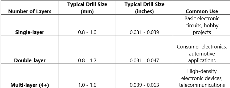
These are tendencies for those two sizes, but then the real size can change depending on the given design requirements and the capabilities of manufacturing. Drilling is one of the essential and most challenging steps while going through the process of manufacturing PCB. So, it is necessary to consult with PCB manufacturers before handing over the PCB prototype in order to pick ideal drill sizes for the present project.
PCBs can be categorized into three main types based on the number of layers
Single-layer PCBs
It was also the time when the term single-sided printed circuit boards (PCBs) appeared. These boards have one layer of conductive material (copper layers) on one side of the board of the copper pads and copper plating. Single-layer PCBs are more often used as a building block for simple electronics that carry rather simple circuitry.
Double-layer PCBs
Also known as double-sided PCBS, these boards are similar to multilayer PCBs, having conductive materials on both sides of the board connected by vias (plated-through holes or plated holes). Dual PCBs are frequently used in many electronic devices, especially when they have to deal with intricate designs and circuit boards.
Multi-layer PCBs
These boards contain a minimum of two or more layers of conductive material placed between an insulating material known as substrate. The layers use vias, which function as the contact between the entities and help with the interconnection of elements. Thinner PCBs are used in high-performance electronics where space is limited and the integrity of the signal is crucial. True, multi-layer PCBs are popular for high-performance electronics.
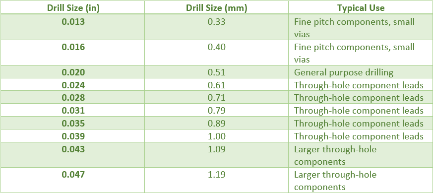
Recommended PCB Drill Sizes
The choice of drill sizes is very important in circuit board design (PCB), because the components are selected to meet that needs and should fit in respective locations while also allowing the board to function as you want it to. Recommended drill size are dependend on such industry standard values and best practices that include the requirement of components size, density,and PCB thickness . Here are some general recommendations for PCB drill sizes:
Fine Pitch Components and Small Vias

For fine-pitched components and small vias, drill sizes such as 0.013 inches at 0.33 mm up to 0.020 inches at 0.51 mm is being adopted. Theses dimensions give the drill the ability to attain accurate drilling into parts.
General Purpose Drilling machine
0.020 inch (0.51 mm from the diameter) is a usual drill size when general drilling time is concerned. This size is commonly used for a large amount of components and applications. This is general.
Through-Hole Component Leads
In case of the through hole components, the rack sizes ranging between 0.024” (0.61 mm) and 0.039” (1.00 mm) are mostly preferred. The pin count value is connected with lead name diameter and PCB board thickness. The specific value may vary based upon these two factors.
Larger Through-Hole Components

For the above-mentioned big through-hole parts, tungsten carbide drill bits can vary between 0.043 inches (1.09 mm) to 0.047 inches (1.19 mm) sizes according to the requirements. These sizes follow the standard packets used for the larger sizes to meet the clearance needs.
The above are general tips for normalization of guidelines for drill size. However, this varies according to the design of the PCB layout as well as the technological capabilities of the manufacturer. Therefore,it is important to confer with your PCB manufacturer and pcb project so that he or she may determine whether the picked sizes are applicable in your design and production process.
Most components have standard lead diameters
Here’s a table outlining standard lead diameters for common electronic components:
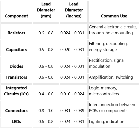
These figures are for nominal diameters and covered only by manufacturing tolerances of components as well as part numbers. The most important thing about PCB layout is to refer the component datasheets to get all the dimension of lead diameter correctly; this will mean proper fit and compatibility.
How to Calculate
It involves figuring out the drill size that suits both the component lead size and the pad size, and also the required annular ring (the inner copper ring surrounding the drill holes). Here’s a general guide on how to calculate PCB drill sizes:
- Determine the component lead size. As far as thickest leads size goes, pick the size that matches your component code. Calculate the diameter of the lead component or search for datasheet of the lead component which will have the lead diameter mentioned.
- Calculate the finished hole size: Add the ring size of chosen annular ring to the component diameter in the round lead. To identify the annular ring size, search for it in your PCB design requirements or use a standard pcb drill sizes like the IPC-2221.
- Finished Hole Sizes = Component Tubing Lead Diameter + Annular Gap Size
- Choose a Drill Size: Choose a drill bit that is about 1/8 inch smaller holes than the minimum hole size you would like to have when the piping is in place. The diameter of the drilled hole must be of the size that would permit the annular ring to fit within the prescribed range of dimensions.
- Calculate the Pad Diameter: Calculate the pad diameter using the selected drill size and the annular ring size that have to be produced.
- Pad Diameter = Drill Size + (2 x Annular Ring Size)
- Check manufacturer specifications: Make sure that the hole size, pad size and/or features area can be produced by your board manufacturer and that you are not exceeding their capacities. In some cases manufacture may define his needs or constraints.
- Adjust as Necessary: Based on the size, kind, and strength of the bolting system that you plan to use, it is indispensable that you may make adjustments in the drill hole size and the pad size.
As is the case with the general requirements, it would be good to point out that the specific challenges are often different for the design. Although there is no way to provide a general recommendation and guidelines as your particular PCB design is unique especially to the electrical components. You can ask a PCB designer and manufacturer for advice.
Tips for Choosing the Right Drill Sizes
When selecting a drill size for a PCB design, consider the following tips:
- Consult PCB Fabrication Guidelines: Generally, the majority of PCB manufacturers supply recordings for drill hole size selection according to their facilities, as well as the design specs.
- Use Design Software: Utilizing design tools will enable you to create an electronic and therefore it will be easy to measure the optimum pcb drills size in terms of your design.
- Consider Component Size: The type size or the components being integrated on the PCB assembly will also have an impact on the pcb holes size of the drilled holes which is needed.
- Think About Future Needs: Prepare for future developments and pick a bit size large enough to allow for further upgrades and modifications in the future.
Conclusion
One of the most vital and non-negotiable attributes when choosing PCB drill size is the production of printed circuit boards that are both professional quality and reliable. The carbide bits are available in compress shank straight bits or straight shank bits formats to the carbide ones. Through following the methods outlined in this guide and keeping informed about the newest innovations and developments, designers can achieve a high level excellence and effectiveness standards of quality and functionality.


