You can find the current developments in and advances for preparing printed circuit boards here. Go and see how technology changes, so that you’ll know its effect on your business. Don’t lag behind the rest. Check out our informative blog first! Dig deeper into where printed circuit manufacture is headed with experts’ analysis. Keep on top of the latest developments, and see how they can transform your business. There is this important information you want to miss?
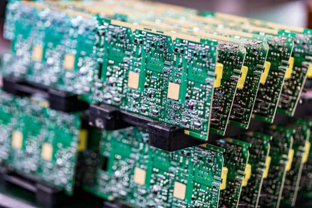
WHAT IS THE PCB MANUFACTURING PROCESS?
The process of manufacturing printed circuit boards (PCBs) is an intricate and significant one in the field of electronics. It involves two key stages – PCB fabrication and PCB assembly. Even though both stages are part of the overall PCB manufacturing process, they serve distinct purposes and contribute to the final product in unique ways.
WHAT IS THE DIFFERENCE BETWEEN PCB FABRICATION AND PCB ASSEMBLY PROCESS?
The process of manufacturing a printed circuit board (PCB) involves two distinct stages: PCB fabrication and PCB assembly.
PCB FABRICATION PROCESS
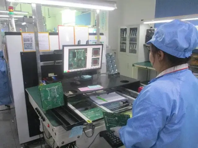
PCB fabrication is the first step, where the real board actually gets made. This all begins with designing the PCB layout, using CAD software. Then you make a board itself. Making a PCB involves adhesively coating one surface of the substrate with copper, etching away unwanted portions to form circuit traces and holes for positioning through-hole components.
PCB ASSEMBLY PROCESS
PCB assembly, on the other hand, follows fabrication and involves populating the board with electronic devices. This consists of mounting the components onto boards, commonly by pcb surface mount technology (SMT) or through-hole technology (THT). PCB assembly includes quality control, testing and in some cases even more steps like conformal coating for added protection.
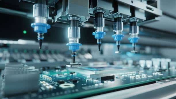
To put it another way, while PCB fabrication is geared to making the physical board itself, in assembly electronic components are mounted on the one made but they being their existence.
Surface Mount Technology (SMT) or Through-Hole Technology (THT)
Mounting electric components to printed circuit boards (PCBs) employs two main methods: Surface Mount Technology. and Through-Hole Techinology.
SMT stands for Surface Mount Techniques, in which components are soldered to the surface of PCB. It uses solder paste and reflow soldering techniques. This method is also quite efficient, it generates smaller components and allows higher component density. Components can be assembled automatically with this approach.
But Through-Hole Technology, on the other hand requires leads to be passed through holes in the PCB. One end is soldered onto one side of PCB and an opposite lead goes into another hole for solder there as well. Mechanically robust and compatible with larger components, HTH is especially selected for those particular applications in which durability and repair work are key considerations.
As to whether it should be SMT or THT, there are several factors that need to be considered: the first is component size; secondly production volume; and finally specific requirements of the electronic device.
WHAT ARE THE PARTS OF A PCB?
Printed circuit boards (PCB), a basic constituent of many an electronic device, are like the motherboards that we stand on and carry our bags.
1. Substrate layer/Base Material
The base material is often called the substrate material and forms a firm foundation for the PCB. Usual materials include the fiberglass-reinforced epoxy resin (FR4), which withstands wear in everyday use better than other common variables, as well as electrically insulating layers of a variety of different varieties.
2. Copper Foil layer
The writable surface of the device is one layer of copper foil laminated onto the substrate material. Electrical signals flow along conductive paths through these traces in a manner similar to that on circuit boards today. To etch away the unwanted copper foil, an inverted image of the desired circuit pattern is engraved upon a thin sheet or sheets of soft metal (copper) beneath it.
3.Pads
Pads are parts of the PCB production surface which were converted into zones for soldered electronic components. They provide a bridge between component parts such as resistors, capacitors or integrated circuits.
4. Traces
However, traces are the conducting conduits on PCBs that lead from one component to another. They are produced using the process of selectively wearing away superfluous copper.
5. Vias
Vias are tiny holes containing a conductive material which join different layers in a multilayer pcb. They carry the electrical signals between different layers.
6. Silkscreen
The silkscreen layer is a printed drill on the PCB which has markings, labels and symbols placed to identify components, reference designators etc. It’s normally printed in white.
7. Solder mask
A protective layer, the solder mask leaves only those parts of copper desired to be soldered exposed so that solvent for brass does not eat away at them. It protects against short circuits and the oxidation of red copper solvent or traces.
8. Components
Solder mask is used to mount electronic components, such as resistors, capacitors and integrated circuits in addition. These elements are the working parts of an electronic circuit.
9. Mounting Holes
Mounting holes are the openings made in a PCB for affixing it to some larger system, like an enclosure or chassis.
10. Copper Pour/Plane
Copper solvent is applied widely in the larger regions of copper pours or planes to furnish a stable electrical ground reference, and to dissipate waste heat from components.
11. Edge Connectors
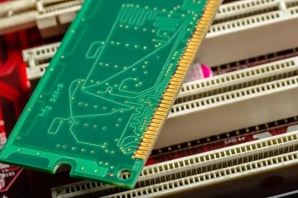
Blade connectors, or more generically known as card edge connectors are a type of electrical connector used to join the printed circuit board (PCB) with an end another PCB but also may be one that is connected to it on its side. The most common use for this equips would electronics such as backplanes and motherboards. Such connectors for connecting PCBs in many electronic devices are widely used and effective.
HOW IS A PCB MANUFACTURED?
The manufacturing of a printed circuit board (PCB) involves several steps, from design to fabrication.
Step One: Designing the PCB
First of all, the printed circuit board (PCB) itself must be designed. This is the most critical phase. Here, using CAD software to draft a very detailed layout of the circuit telling where components and traces, vias et al are placed can take several days or even weeks. To achieve proper functionality and efficiency, designers work to general guidelines along with a number of considerations.
This design process produces digital data representing different levels of the PCB, which act as reference materials for follow-up steps such a production work and film printing. From there comes layer lamination, before finally being turned into to actual board. The precision and accuracy of the PCB’s design lie at root to manufacturing functionally effective electronics, let alone whether that happens in-house or OEM.
Step Two: Design Review and Engineering Questions
After the initial design of a printed circuit board (PCB), there is also an intense review and resolving technical questions.
What challenges ahead The critical phase involves intensive scrutiny of the PCB layout, including component positioning, signal integrity requirements (signal lead length), thermal management and manufacturability of manufacturing pcb. Design feasibility and performance/efficiency layouts are worked out.
This step usually includes asking technical questions of the design, and answering them so as to further refine it before moving onto production. During this phase, communications and solving problems must be effective. Doing so promotes a smoother-running production process without errors in the PCB board itself when it finally comes off of the assembly line meeting specifications for standards.
Step Three: Printing the PCB Design
The third step in PCB manufacturing is printing the design, following the review and improvement of it by means of a formal design meeting.
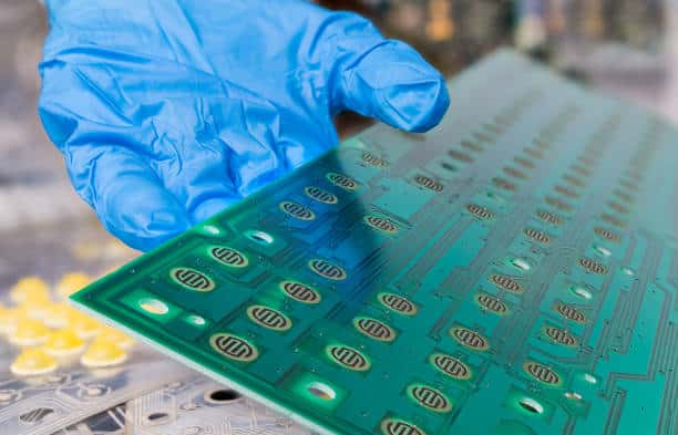
This stage makes films to represent the different layers of PCB from what is detailed by design. These films are part of the process for transferring the circuit pattern from film to board. A coat of a photoresist material is coated on the copper clad substrate, and the various films are used to selectively expose certain areas. After development and etching the exposed areas are produced as traces that form to required specifications.
Printing Thirty five thousand of these bearers are printed, making this process an important step in the translation from digital design to physical layout for PCB. After all, only after printing can drilling and component assembly begin.
Step Four: Printing the Copper for the Interior Layers
At the fourth stage of production in printed circuit board (PCB) making, one works on printing the copper for internal layers. It is the bonding of copper foil to substrate which creates those conductive layers on Sheet. The copper carefully applied to the surface sticks closely to its prescribed circuit pattern designed earlier.
Next, the layers are put through a lamination process to fuse them all together. This gives it a multi-layered structure. This step is essential to the establishment of the conductive paths that make up a circuit. This stage demands high precision printing of the copper layers, and it makes an important contribution to performance in actual operation.
Step Five: Etch the Inner Layers or Core to Remove Copper
The fifth step in the manufacture of printed circuit boards (PCBs) is to etch away anything outside the required finish the copper layers. The next step involves laminating the copper layers onto the substrate. Unwanted, remaining pieces of this layer are then removed by means of chemical etching in fabricating process so that only what’s actually needed remains in its place which this steps will removes the excess copper.
This step is essential for precisely laying out the circuit traces on the interior layers of PCB. The areas covered by that previously applied photoresist persist, forming the conductive paths which are part of the circuit. In order to replicate the intended circuit pattern accurately, it is essential that precision in etching run through every step of the process. When done, the PCB proceeds to operations such as drilling and solder mask application.
If a Printed Circuit Board Manufacturing Process Is for Multilayer Designs
But when PCB-manufacturing requires multilayer designs, it adds complexity and another knowhow to the already standard procedure.
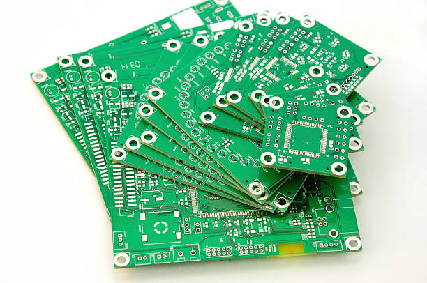
However, multilayer PCBs have more than one layer of conductive material sandwiched between layers of insulation. The result is a much richer circuitry scheme. Printing and etching layers is done one by one, then they are stacked to form a whole. Here tight alignment and registration of the various layers are needed. Also, vias–tiny holes that connect the several layers of foil are added.
Electronic circuit manufacturing requires absolute care to get the correct design produced and create an unimpeachable, fully-functional product.
Inner Layer Imaging
The third stage of printed circuit board (PCB) manufacture is inner layer imaging. Here, it’s all about transferring the pattern onto the inside layers of the plywood stack up.
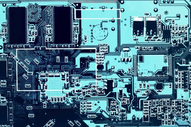
The copper-clad substrate first must be coated with a thin layer of photoresist. This is then exposed to the UV light contained in an enclosure, and the circuit design has acted as a template for this process. The exposed areas solidify, while the unexposed regions remain soluble. The circuit patterns are then followed by development and etching, which remove all the remaining unexposed copper.
This process is thus essential to the defining of conductive paths on the inside layers of a PCB, and having laid this foundation then begins building an accurate, effective functional electronic circuit. The impression made by the inner layer imaging process has a great effect on the quality of the entire PCB.
Inner Layer Etching
During the in input layer etching of printed circuit board (PCB) manufacturing, the aim is to selectively remove excess copper from the inner layers. After a photoresist layer is applied onto the insulator according to its circuit design, and UV light irradiations are done on it, only those parts exposed by the ghost mask will be selectively developed before being etched.
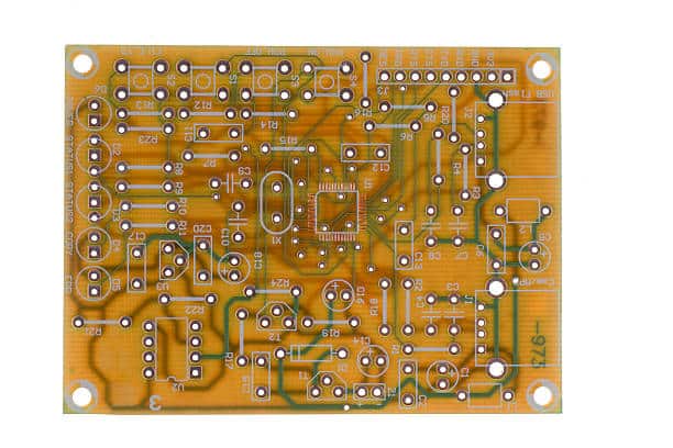
This chemical etching removes the exposed copper, leaving behind only that which has been defined by this particular circuit design. inner layer etching is another important step in forming the conducting tracks on a PCB fabrication process. It subtly replicates all those delicate circuits with absolute accuracy. This process requires extreme precision for the electric circuits to operate properly and smoothly.
Resist Stripping
The stripping step is a critical part of the PCB manufacturing process in which any photoresist material still left over from earlier stages must be stripped. The last step in processes such as inner layer imaging and etching is to leave a coat of photoresist on the surface. This residual photoresist must be resisted away. One technique is to apply a solution that dissolves this unwanted product, leaving behind the exposed copper traces intact.
This is intended to make sure that any undesired objects will be gone, so as not cause potential problems such as short circuits. This step keeps the PCB clean and also assures it is in pinpoint condition. It establishes a good foundation for subsequent processes such as solder mask application and component mounting.
Post Etch Punch
During the PCB manufacturing process, post-etch punch is a critical step. When inner layers have been etched (a process that exposes the copper foil), precise holes or perforations must be punched into it as part of this stage in production which looks at penetrating through to particular parts on another layer beneath soas to produce desired effects such as connections between components and ground imm These holes exist for various reasons, such as providing points of reference during subsequent lamination processes on multilayer PCBs or allowing machine make drilling hole a and b.
The post-etch punch keeps the dimension accurate and assures proper alignment of component on PCB. It helps to ensure a good quality, reliable final electronic circuit.
This step is especially critical in the production of multilayer PCBs. Registration here is very important, and it must be accurate to ensure that layers align during lamination.
Inner Layer AOI or Automated Optical Inspection
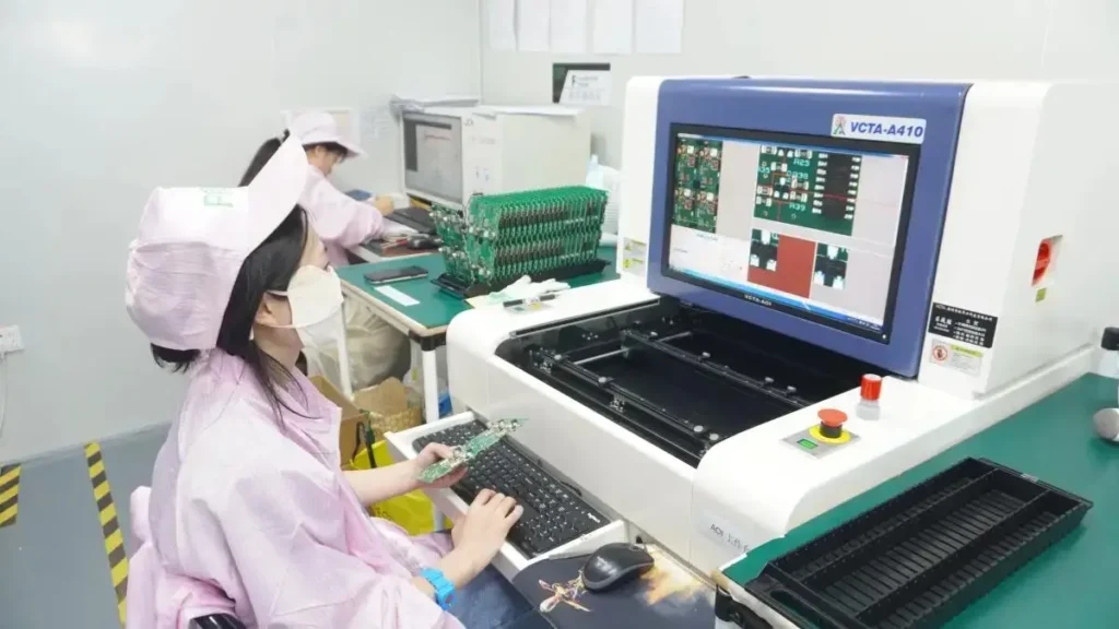
The print inner Layer Automated Optical Inspection (AOI) is a critical step in the printed circuit board manufacturing process. It involves using advanced optical systems to identify problems and imperfections on the inside layers of the board.
Advanced algorithms and cameras are used to scrutinize the circuit traces, vias, etc. Commercial products based on this technique have been introduced by Xerox. It also finds potential problems–it detects whether components are missing, misaligned or incorrectly soldered and if any part isn’t up to design specifications.
AOI of Inner Layer not only tests and ensures the quality and precision, it also guarantees itself to be rapid in examination as well thorough. That assures all links being firm throughout is essential in making sure reliability over every wiring trace on complete PCBs finally seals into reality for total electronic circuitry.
Inner Layer Oxide
After etching, the exposed copper is then encapsulated in an oxide film. Formation of this inner layer (oxide) constitutes a major part of PCB manufacturing technology.
This layer plays the role of a protective shell and is critical to maintaining the integrity of copper traces. It prevents oxidation from occurring before they reach later production stages. The inner layer oxide brings better solderability and aids the adhesion of other materials, which leaves it with high overall durable.
This oxidation prevention step is vital for maintaining the conductive qualities of the copper traces, so that later (after assembly) both it and its surrounding environment will function properly long term.
Layup
That is what layup refers to in the printed circuit board (PCB) manufacturing process, which involves stacking and aligning various layers that collectively form a multilayer PCB. The layers, including all of the internal ones with circuit traces, are organized and laminated together to form a single structure.
Given how intricate multi-layer PCBs tend to be, this process requires precision in order for a given layer’s registration and alignment with the preceding (or following) one unfailingly to fulfill its function. Layup provides the foundation for subsequent bonding, so that an integrated board structure with adequate strength to bear its electronic circuits can be developed.
Lamination process
The lamination process is an important step in manufacturing printed circuit boards (PCBs), especially for multi-layer types. This process occurs after layup, where individual layers are stacked. It involves consolidating these layers through the application of heat and pressure. After applying heat to the board, melted prepreg material flowing between copper-clad layers bond with and fill in crevices to produce a solid slab.
When the lamination is done, you have a solid multilayer PCB with clearly defined conductive pathways. This is an important step for the realization of electrical performance, structural integrity and reliability required of a high quality electronic circuit in the end.
X-Ray Alignment
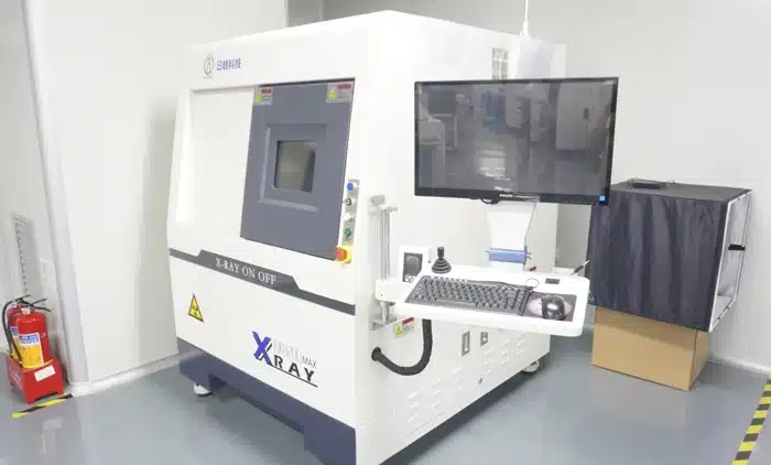
In the printed circuit board (PCB) manufacturing process, because of its special structure X-ray alignment plays an important role in multilayer PCBs.
With this technique an X-ray camera is used to check and maintain the correct positioning of layers inside a multilayer stack. The X-ray images can be utilized to ensure proper registration for each layer, as well as identify any misalignment or deviations. In multi-layer PCB’s, in particular those with several layers, aligning X-rays is a must to retain the accuracy of their intricate circuitry.
By removing these possible problems beforehand during the manufacturing process, this quality control step greatly increases the general usability of both function and performance for your PCB.
Step Six: Layer Alignment
In the sixth process step in printed circuit board (PCB) manufacturing, layer alignment is star attraction. The most critical period is during the precise alignment of each individual layer. All such layers must be assem-bled with their conductive patterns and components in exactly correct positions. For multilayer PCBs, where the circuitry is very intricate and compact, accurate layer alignment becomes a basic necessity.
The boards are piled up in a meticulous manner, with alignment marks or points of reference being used to align them. This step creates a firm foundation for subsequent operations including lamination, and thus is an important factor affecting the accuracy, reactivity along with reliability of finished electronic circuits.
Step Seven: Automated Optical Inspection
AOI is an automation that plays a vital role in the seventh step of printed circuit board (PCB) manufacturing. In this fully automated and high-tech inspection method, optical systems combined with advanced algorithms carefully inspect the PCB for flaws. One scrupulously accurate result of quality control is that the circuit patterns are now highly integrated; another more convenient one: Waypoint micro assembly can also be used to put parts on or off a motherboard pcb design.
Potential problems include missing or misaligned parts, solder defects and violations of design specifications. AOI finds them all. The automated inspection speeds up the process while increasing accuracy by quickly finding any defects in manufacture, and so improves overall quality assurance for entire electronic circuit board.
Step Eight: Laminating the PCB Layers
Step Eight-Lamination of PCB Layers The attention is on the layers that make up the printed circuit board (PCB).
This all-important phase then subjects the individual layers of the PCB to heat and pressure in order that they can be welded together. After applying heat to the prepreg material between the copper-clad layers, it becomes active and is next turned into a unified multilayer structure. Adding lamination as the final step makes a PCB laminating process sturdy and with clearly-defined conductive pathways.
This step is crucial because it determines the needed electrical performance, structural integrity and overall reliability of this circuit as an electronic device.
Steps Nine: Drilling
Drilling is the ninth step in manufacturing a printed circuit board (PCB). However, it is an indispensable stepin which holes are precision-drilled through the PCB. Not only do these pilot holes provide places for placing components but they also form connections between different layers of the board.
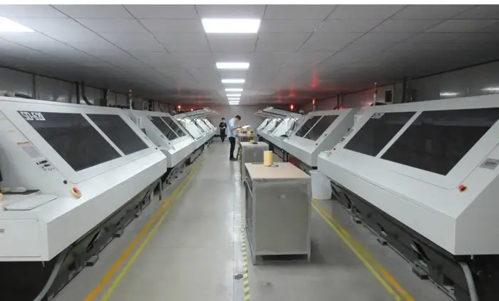
Because these drilled holes are called vias, the resulting multi layered structure is formed. Precise DrillingEfficient embodiment of subsequent processesAccurate drilling is indispensable to proper alignment and connectivity, being the precursor for plating as well as component assembly. Shaping the PCB for integration of electronic components, and letting signals flow through adjacent circuits throughout are two key steps.
Steps Ten: PCB Plating and copper deposition
Plating and copper deposition are the tenth step in manufacturing a printed circuit board (PCB). This step involves plating the drilled holes, or vias–also known as through-holes–inside it with a thin film of conductive material such as copper. It is the plating process that increases contact between different PCB layers, ensuring complete electrical connectivity.
It also stiffens the sides of vias, increasing the strength of the entire board. Copper deposition is an important step in preparing the PCB for subsequent operations of component assembly and soldering. It is critical for the integrity and function of an electronic circuit that this plating process requires such a high degree of precision.
Step Eleven: Outer Layer Imaging
The eleventh stage of the printed circuit board (PCB) manufacturing system centers around outer layer printing. This critical stage is called transferring the circuit pattern onto the outer layers of the PCB. The outer layer imaging process is basically the same as for inner layers. A photoresist coat similar to that on other sides of copper-clad substrate is put down upon which circuit design again exposes through UV light.
Later development and etching remove the unexposed copper, leaving behind thenet circuit traces on the outer layers. You need outer layer imaging to mark the conductive passages on both sides of the PCB, after which you can apply solder mask and finish a complete set of components. Precision in this step assures effective reproduction of the circuit pattern on outer faces that he has designed into the PCB.
Step Twelve: Outer Layer Etching
The printed circuit board (PCB) manufacturing process includes a twelfth step dedicated to etching the outer layers. Exposing the excess copper on the outer layer This step relies on selectively removing excess copper at areas of exposure for surfaces to be exposed among these layers.
During imaging, the photoresist layer protects the circuit traces. Only excess copper is removed by etching away from it. The outer layer etching step is important, since it smooths the circuit pattern on both sides of the printed board. Afterward comes application of solder mask followed by component installation and testing (the latter generally forms one process). In this process, accuracy is critical for the electronic circuit’s precision and continence.
Steps Thirteen: Outer Layer AOI
Outer Layer AOI begins in the thirteenth step of PCB manufacturing. An automated inspection This technique uses high quality optics and calculation techniques to completely inspect the outer layers of these PCBs for flaws. Its inspection of items like circuit traces, soldered joints and components ensure that they conform to the design specifications.
Quickly detects and responds Outer Layer AOI by finding potential manufacturing defects early on, thereby increasing efficiency for the entire production flow. It also enhances quality assurance of final electronic circuit applications. This step is an important one in ensuring that the PCB remains both precise and reliable, before entering subsequent stages of component assembly or soldering.
Steps Fourteen: Solder Mask Application
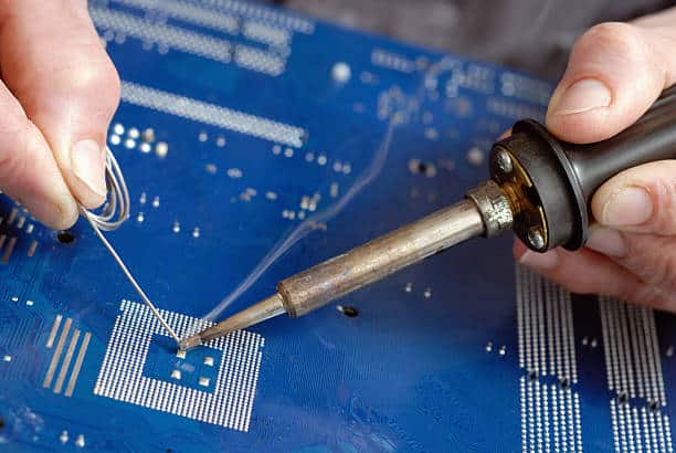
In the fourteenth step of printed circuit board (PCB) manufacturing, attention turns to solder mask application. This important step includes the application of a protective coat, called a solder mask, over the surface of the PCB. Its purpose is to cover the circuit traces with the exception of those areas into which components are soldered.
It protects the PCB from environmental factors, while also preventing solder bridges. The overall reliability of the board will increase. PCB Production Solder mask application is the last of a series of operations that, cumulatively with the others (drilling, plating-etching and silk screen printing), are necessary to yield completed electrical boards. Precision is important for this step, as it influences the optimal functioning and lifespan of the PCB fabrication process.
Step Fifteen: Silkscreen Application & Surface Finish Application
From the fifteenth step in PCB manufacturing, attention shifts to silk screen and surface finish application. During the silkscreen process, data markings including component designators and part labels are printed on the surface of a PCB. This step aids assembly and troubleshooting. Meanwhile, surface finish application, a zinc coating applied to exposed areas of copper in order (a) improve solderability and (b) prevent oxidation.
These finishing touches add to the ease of assembly and quality assurance, along with practical functionality. Whether it is for silkscreen or surface finish applications, the precision in both must ensure a printed circuit board that has well-marked outer edges and resistances strong enough to make it truly durable.
Step Sixteen: Finishing the PCB
The printed circuit board (PCB) manufacturing process consists of sixteenth and final step, polishing. It is all about finishing touches to make sure the PCB meets quality standards so that it can be assembled into electronic devices. Comprehensive testing This stage includes confirming that the design of the PCB meets specifications and quality standards. Necessary adjustments and corrections are made; the finished PCB fabrication process is then given final inspections.
With this step we reach the end of complex manufacturing, and end up with a finished product-a fully functioning, reliable board that can handle anything from home appliances to mobile computers. In the finishing step, handwork should be intense: This meticulous attention to detail is absolutely necessary for providing a high-quality product that meets modern electronics needs.
Step Seventeen: Electrical Reliability Test
The seventeenth step of the printed circuit board (PCB) production process involves inspection to ensure electrical reliability. One of the most important aspect is this stage in which all thoroughly inspected completed PCB boards are put through a circuitry test, guaranteeing their quality and accuracy to pcb design specifications.
The test for electrical reliability is an indispensable step to check that the PCB operates normally and meets the specified level of quality. With so many requirements, the uniform standard for electronic circuits undergoes such a rigorous evaluation process that we can have confidence in their reliability and performance before integrating them onto a printed circuit board.
Step Eighteen: Profiling and Route Out
As for profiling and route-out, it is part of the eighteenth step in manufacturing printed circuit boards (PCB). Profiling means cutting out a finished-sized PCB outline. This step is to ensure that the size of the board conforms with intended specifications, so that it can be used on its target electronic device. Compared with the former, route-out involves things that fall across several boards on a panel (including areas between individual chains or stacks of boards) being chipped away.
Profiling and route-out are necessary for shaping the PCB precisely so as to make it easy on integration within a target electronic application. These last steps in particular require great precision, all of which contributes to the finished printed circuit board’s function and appearance.
Step Nineteen: Quality Check and Visual Inspection
This step still demands strict quality control procedures in order to provide printed circuit boards with high performance and good reliability.
The nineteenth step of the printed circuit board (PCB) manufacturing process focuses on quality checks and visual testing. The crucial stage: Thoroughly inspected When the PCB is complete, it must be carefully checked for any defects, anomalies or irregularities. Quality checks involve many elements, including solder joints, component placement and overall board strength. PCB inspection needs to guarantee that the design and manufacturing standards are met.
Step Twenty: Packaging and Delivery
The twentieth and final step in printing circuit boards is to focus on packaging and shipping. When PCBs are successfully manufactured by going through the various stages of production and pass inspections for quality, great care is taken in packing them up so that they will not be damaged during transport. Board packaging methods are prepared to avoid damage and ensure their integrity. Once securely packed, the PCB manufacturing process flow are ready for delivery to end users, electronic device manufacturers or assembly plants.
These final steps make sure that the carefully produced and quality-checked PCBs reach their destination in flawless condition, ready for nearly every type of electronic application.
HOW TO IMPLEMENT AN EFFECTIVE PCB MANUFACTURING PROCESS
Making the printed circuit board (PCB) manufacturing process efficient and effective requires planning, precision and being in line with industry standards. Designing typically starts out very comprehensive, with computer-aided design (CAD) software used to create a PCB layout that meets the electronic application’s specifications. To solve any engineering problems and to make the design more suitable for manufacture, both design and manufacturing teams must work together. Each production step, from substrate preparation to final packaging must be clear and efficient. Also very important are quality-control measures, such as automated optical inspection (AOI) and electrical reliability tests to identify defects.
In the successful PCB manufacturing process, regular training for personnel, continuous improvement of processes and adherence to environmental and safety standards are also important elements. Communication and collaboration throughout all phases of production are critical success factors, making possible the high-quality reliable printed circuit boards required for electronics diverse applications.
Components
In electronic circuits, components are the basic elements which perform specific functions. Many different kinds of devices, from resistors to integrated circuits. Resistors regulate the flow of electrical current, capacitors accumulate and discharge energy in electrostatic fields. Inductance stores electricity as a magnetic force field; transistors amplify or switch between two contacts (high impedance); integrated circuits combine various functions into one box.
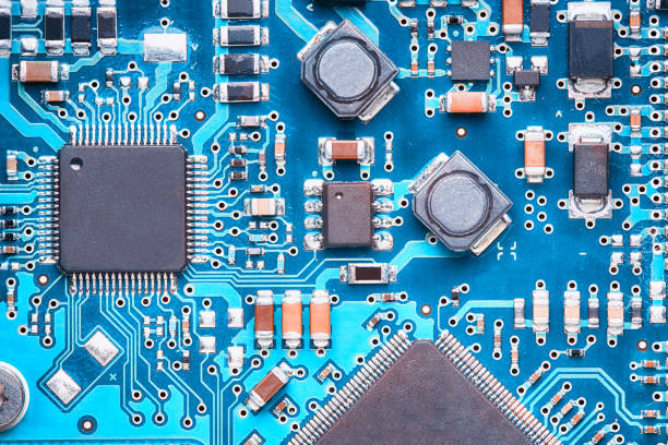
Electronic circuits are achieved by interconnecting the components on a printed circuit board (PCB); choosing, placing and integrating them properly is an important part of getting electronic devices to function well.
Design for Manufacturing (DFM) Considerations
Optimizing the design for efficient and cost effective manufacturing Design for Manufacturing (DFM) is very important principles during product development. The approach focuses on designing products so as to reduce assembly, increase quality and lower costs.
DFM includes factors such as material choice, component location decision, ease of assembly and manufacturability. DFM, which helps manufacturing teams identify and solve potential problems before the design is sent to pcb fabrication assists in reducing defects; improving product reliability; and decreasing lead times for production. Applying DFM concepts allows design and manufacturing teams to cooperate closely, so that the transition from initial ideas through designing eventually leads to high-quality products at reasonable costs.
File Formats
In the case of printed circuit boards (PCBs), file formats are important for transferring design information from one stage in the manufacturing process to another. Gerber files are one of the standard formats used in PCB design, and contain information on copper layers, solder mask & silkscreen elements. An Excellon file describes the location of holes drilled into a PCB. Also, Extended Gerber (RS-274X) has also become standard format which contains various types of data required in the pcb fabrication and assembly processes modern PCB.
The file formats guarantee an accurate telephone representation of the PCB specification and smooth information exchange between design software, CAM (Computer-Aided Manufacturing) systems for pcb fabrication equipment.
Board Materials
Board materials are important ingredients used in the making of printed circuit boards (PCBs), determining their characteristics and performance. Combined with materials such as fiberglass-reinforced epoxy, the substrate provides structural support for the PCB for the printed circuit board assembly.
Copper layers are finally added to the substrate, creating conductive pathways for electrical signals. For example, one important factor in determining PCB characteristics such as signal integrity or heat dissipation is the selection of board materials bare board. Some advanced choices include high-frequency laminated boards and flexible substrates.
Selecting materials The selection of PCB materials is made with the particular requirements of a given electronic application and ensuring that the PCB meets performance standards in mind to finished board.
