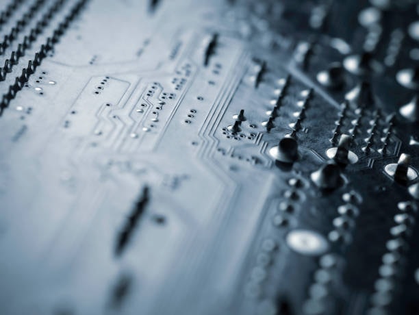
Printed Circuit Boards (PCBs) are the central parts of electronics devices; they act as a base to hold electronic components and act as conductors for the connections. A key process particularly for through-hole components is solder paste deposition and stencils are used during this process. This guide is specifically written for the new users who need to know basically all about stencils used in manufacturing of PCBs, including types, materials, and ways of stencil production and application.
What is a PCB Stencil?
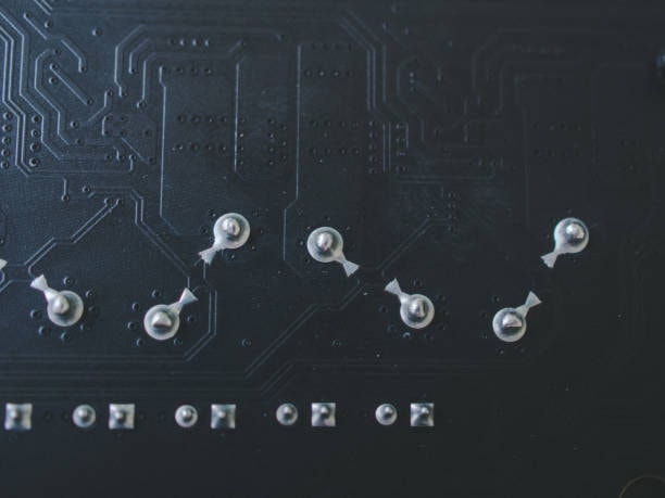
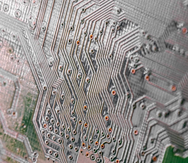
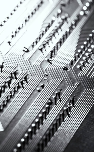
PCB stencil or the solder paste stencil is some type steel sheet of a thin sheet or foil that has aperture on it. These openings are the areas that require the paste to be deposited on the PCB. Stencils are mainly used for Screen Printing Technology to achieve consistent deposition of solder paste to the pads of the PCB for ease in mounting of surface mount-device during Reflow Soldering.
Types of PCB Stencils
There are several types of PCB stencils, each designed to cater to specific requirements and production volumes:
Frameless Stencils
These are elastic and simple in handling.
Mainly used for developing prototypes and in the production of relatively low quantities of goods.
Affordable and can be stored.
Framed Stencils
- Suspended on the frame to get enhanced stability and strength .
- Most suitable when the production run is bighted for high volume production runs.
- Have higher accuracy and reliability.
Electroformed Stencils
- An electroformed piece that was created to reflect the characteristics of the material used.
- Deliver good aperture definition and, at the same time, fine-grain structure/texture on the walls.
- Applicable to narrow leads or WLCSP packages and thin substrate height assemblies.
Laser-cut Stencils
- Cut on state of the art Lazer cutting technology.
- High precision and accuracy.
- Typically applied in both the development of the initial model and series production.
Materials Used in PCB Stencils
Consequently, the selection of the PCB stencil materials will determine its capacity regarding flexibility, consistency, and durability reusable stencil frames. The most commonly used materials include:
Stainless Steel wire mesh
- Its delivery is very high where strength is a much sought after property.
- Applicable to small and large scale production or manufacturing business.
- It gives uniform and accurate solder paste deposition.
Nickel based stencils
- Used in electroformed stencils.
- Delivers improved sharpness in the perimeter of the aperture and improves the surface’s comparative flatness.
- Perfect for fine-pitch and high-density of the printed circuit boards.
Polyimide
- Flexible and lightweight.
- It is widely applied in the prototype and small batch manufacturing.
- Offers good results relative to the metal-etched stencils but has shorter working life than the ones made of metal.
The Stencil Creation Process
The process of creating a PCB stencil involves several steps, each contributing to the accuracy and quality of the final product:
Design Preparation
Pads for the laser stencils are also generated from the PCB layout.
The stencil aperture size patterns are designed by CAD software and it depends on the PCB pads of it.
Material Selection
Based on the production requirement an appropriate material out of stainless steel, nickel or polyimide will be used.
Cutting
Laser Cutting: These lasers precision cut the apertures of the stencil material thus giving it high precision cuts and very sharp edges hybrid pcb stencils.
Electroforming: A nickel layer is built up on the substrate by electrolytic deposition and the geometrical cross section of the apertures obtained can have smooth walls.
Cleaning and Inspection
The stencil’s surface is washed to eliminate even smutty and particulate pollutants so that molten flocculant can cover the surface well.
This checking is done so as to ensure that the apertures are correctly located and have no visible blemishes.
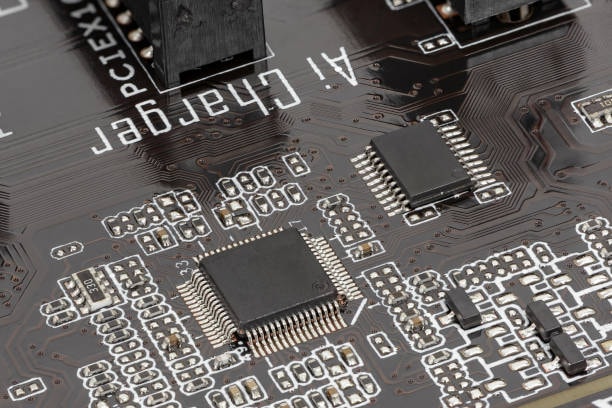
Using a PCB Stencil in Assembly process
Using a PCB stencil in the assembly process involves several key steps to ensure proper solder paste application:
Stencil Alignment
The stencil is registered with the PCB to make sure that the apertures correspond with the pads on the PCB.
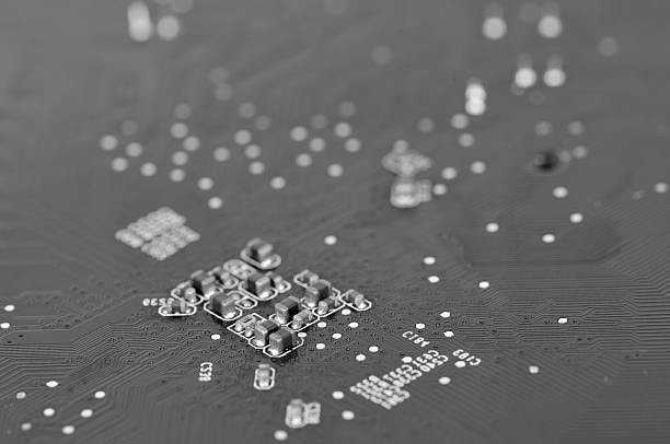
Solder Paste Application
Solder paste is printed on the two smt stencils and then it is in contact with the PCBs through the application of certain pressure to force the solder paste through the holes in the stencil frameless pcb stencils.
The paste goes through the weaves and dispenses on the PCB pads.
Stencil Removal
Solder paste is accurately placed on the pad where the stencil is peeled off from the PCB very slowly.
Component Placement and Reflow
Component Placement and Reflow Soldering
SMT components with leads are placed onto the solder paste.
The PCB is then taken through a reflow oven where the components are connected through the solder paste and good solder joints surface mount components are made.
Advantages of Using PCB Stencils
Using stencils in PCB manufacturing offers several benefits, including:
Accuracy and Consistency
This decreases the chances of various types of defects, especially on components such as stencils where high accuracy in the amount of solder paste and deposition is desirable.
Efficiency
Stencils help in speeding up the process of solder paste application and this is likely to enhance production smt stencil.
Cost-effectiveness
Prevents problems that are associated with solder paste usage; thus, eliminates the need for contractors to spend a lot of money on solder paste that has been timelessly178 smeared on and around circuit boards, only for them to be returned to the manufacturer and redone.
Improved Reliability
Provides highly dependable solder joints which directly improve performance and durability of the final assembly on printed circuit board.
Common Challenges and Solutions
Although the research shows the advantages of using PCB stencils, it is also important to note that doing so can also pose some certain difficulties pcb board. Here are common issues and their solutions:
Misalignment
Solution: To check stencil thickness and alignment, it’s recommended to use alignment fixtures and other precise equipment.
Solder Paste Clogging
Solution: Maintenance is required for the stencil apertures and you should always apply good quality solder paste of right viscosity.
Stencil Wear and Tear
Solution: Stencils should be selected from sturdy material such as the stainless steel and they should be checked frequently and replaced on as often as required.
Insufficient or Excessive Solder Paste stencils
Solution: Apply the correct pressure and angle from the squeegee taking into consideration consistent Solder Paste Deposit.
Innovations in PCB Stencil Technology
Technological advancements in the aspects of the manufacturing of PCB stencils yields improvement of the manufacturing process. Some notable innovations include:
Nano Coatings
Solder paste release or clogging hence, stencils have been developed with coatings made of nanomaterials.
Automated Stencil Printing
Combined usage of laser stencil technology for printers with pick-and-place machinery in the most effective and appropriate method.
Advanced Materials
There seems to be a need for advancement in the fabrication materials that are used for constructing high density as well as fine pitch PCBs.
Conclusion
PCB stencil is an indispensable item the assembly because it assists in the application of solder paste on circuit boards in the right and standard way. Some of the things that may be so useful to the new comers in PCB fabrication include the following; Classification of stencils, Material used in its construction, The process of construction and at last the usage techniques. Thus, the use of stencils helps to produce better-quality and more reliable PCB assemblies, and at the same time increase the speed of production.


