Understanding the printed circuit board (PCB) stack up is crucial for designing and manufacturing high-quality PCBs. Learn about the importance of PCB stack up and key considerations in this comprehensive guide.
What is Stack-up?
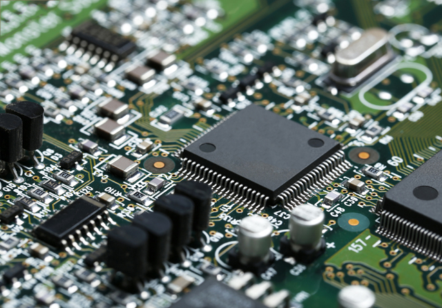
We must know first what is the meaning of Stack up. Stack up means is to locate and arranged those various pcb layers. Moreover, the use of many layers or those components in order to accomplish the desired design rules or functions to the common occurrence to those many disciplines such as electronics, the manufacturing, the engineering and those electrical and computer sectors.
As you can see the printed circuit board design requirements. You see the picture above the stack up which have the process of arranging those different layers elements such as the copper layers and insulating layers which is to form a the circuit that have both functional and dependable.
Another precise definition of stack up especially in manufacturing which this is the way for dimensions and tolerances are being organized in the product design rules which in order to guarantee the called good fit and have efficient operations. Also, When you are describing a structure to those parts are being arranged by layer stack or vertically you can see the word “stack up” is frequently employed.
THE PURPOSE OF PCB LAYER STACKUPS
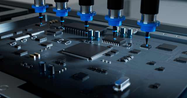
What would be the purpose of the Printed circuit board layer stack ups? In this part we will know a very comprehensive explanation regarding about the purpose of stack up. We will begin.
The main purpose of Printed Circuit Board layer stackup is the arrangement and pcb layout in those various layers in pcb stack in order to achieve those specific materials such as mechanical, the electrical and thermal properties. And the PCB layers stack up it really play the important role when govern the board thickness performance, signal integrity as well as the functionality.
To reduce electromagnetic interference, power plane, ground planes the engineers can control the impedance control as well as optimizing the board’s thermal management. Reliable signal layers transmission with those minimal interference was being achieved by the layer stackup, which it makes it very easy to route traces signals, vias and components, signal transmission.
OBJECTIVES WHEN CREATING A MULTILAYER PCB STACK ups
By identifying those objectives while creating a multiple layers pcb stackup design that will aims for the optimal electrical performance, those reliable signal layers integrity and the efficient thermal management, which is the strategic layer stack is the engineers goals different types in order to:
1. Optimizing Signal Integrity
The first objectives is that the place signal, the power and the ground planes engineers should take good care or carefully control impedance, they should minimize the signal distortion, and it should be ensure the reliable signal routing transmission across the board.
2. Manage Thermal Considerations
The stack up should have a design in order to have efficient dissipate heat generated by it components, the engineers should make sure that the Pcb layer stackup operates within the safe temperature limits either High temperature or low.
3. Facilitate Power plane Distribution
As an engineer you should arrange the power plane in order to have a stable and efficient power dealing out network, and especially minimize voltage drops or minimize radiation and to ensure the consistency of the power delivery time.
4. Minimizing Electromagnetic compatibility (EMI)
To this the EMI should be properly ground planes and shield should be sensitive components in order to reduce the Electromagnetic compatibility and also to fully aware the interference with those other parts of the circuit or the external noise devices.
5. Simplify Routing and Components Placements
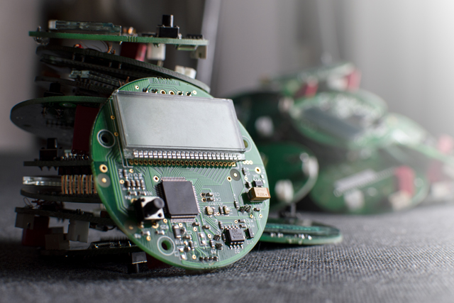
By creating a stack up that will surely allows for the high quality of routing of traces and the vias while obliging the placement of the components in order to meet the layout requirements stacked and ease of assembly.
6. Meet Cost and Manufacturing Constraints
In this objectives you must consider the production costs suggestions in your chosen stacked in terms of the materials you used, the fabrication of complexity and the manufacturing process.
7. Ensure Layer – to – Layer alignment
You should maintain the accurate and precise layer stackup for registering in order to avoid misalignment issues when fabricating, and it could also lead to the performance and reliable issues.
OTHER FACTORS TO CONSIDER WHEN CREATING A MULTILAYER PCB STACK
It was being mentioned in the article about the primary objectives, that there are some other factors that the engineers they must consider when they creating a multiple layers of Pcb stack ups:
1. Materials selection
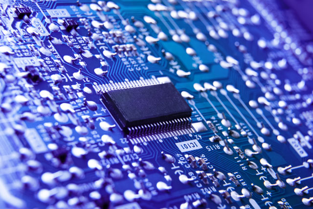
In picking the best suitable under layer stack of materials with the right dielectric material, thermal conductivity, and other dielectric materials properties in order to see the specific needs of this application.
2. Impedance Matching
By ensuring the proper bar by matching for the critical signal layers traces and the layers count to aware the signal reflection as well as by maintaining the signal integrity.
3. Layer Count
By regulating those have optimal number of layers found by the complexity of the circuit example to considered the factors for example the signal density, power distribution and production costs.
4. Blind vias and Buried vias
By evaluating those needs for the blind vias and buried vias is by enhancing the routing options as well as by reducing the layer pcb transitions, but you need to be more mindful because of the impact on those fabrication process and the layers cost of it.
5. EMC performance or EMI performance
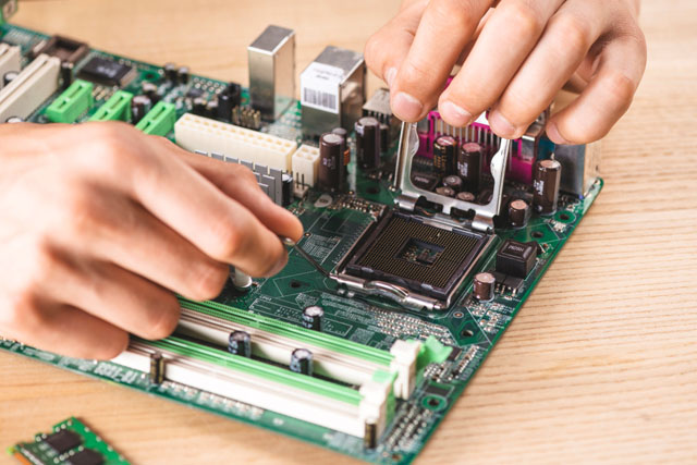
The design requirements of the stack up by complying with the electromagnetic compatibility (EMI) power standards, by minimizing the difficult structure to interference with other electronic devices wither long term reliability or have a board density.
6. High speed signals and RF considerations
Those account for this high speed signals and also the ratio frequency design for example the signal integrity, inner layers, multilayer boards or multilayer pcbs as well as to minimized the transmission line impact.
7. Thermal Relief for Ground planes
By implementing the thermal relief patterns in gnd plane is by facilitating the soldering of signal layer and thermal expansion in order to have improvements the manufacturability.
8. Manufacturability and Yield
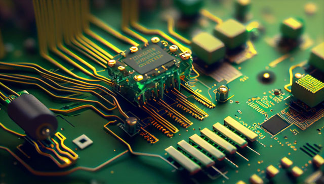
Optimizing the stack up for no trouble of manufacturing is to consider the fabricated process, the tolerance either outer layers or surface layer stack up and have the potential dispute by enhancing the yield.
9. Layer Symmetry
The goals for this symmetry in those many layers stack up is by promoting the even thermal distribution and by also minimizing it during the manufacturing.
To have the better and unique balance for these is by ensuring the multiple layers of the layer pcb stack which either you can meet the standard of the material requirements of the applications.
COMMON TYPES OF PCB LAYER STACKUPS
We have common various types of PCB LAYER STACKUP which is it will refer to standard configuration of layers in pcb by each of the following served as the specific purposes. for example:

2-Layer stackup
Composed of a many layer such as the top layer and bottom layer.
Suited to a simple circuits which have a minimal complication.
4-Layer stackup
We have here many layers such as the two signal layers and two internal planes which are the power and gnd plane.
It also provide to improved the signal integrity and have a better pcb power distribution compared to two layer board thickness.
6-Layer stack
In 6 layer pcb it give additional signal layers and ground layer in order to increased routing or higher yields suppleness thickness.
And the best thing when it comes to ideals material such as the design complex, high speed signal layer, as ell as by improving the power distribution of the.
8-Layer stack
This layer it will give and provide more long term reliability and it will add another signal and gnd plane.
The best thing for this when it comes to ideal designs for complex, high speed signal layer and it improved the power distribution.
10-Layer stack
The layer density will further offer for it to intricate the designs with multiple high speed signals.
Also the ten layer will also provide by enhancing the control over emc performance and reduce the signal crosstalk.
What is Ball grid array?
When we say bga components it is known as to used in those modern electronics by providing those reliable and compact solution for integrated circuits and also those applications in bga components where spacing and the thermal considerations critical.
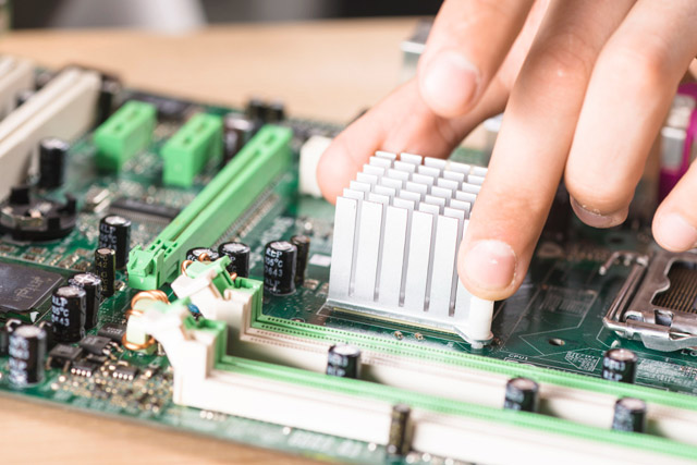
Stack-Up Requirements
1. Layer Arrangement
To identify by arranging of the signals, power as well ad the gnd plane in pcb.
Identifying those order and the different types of layers in order to meet the goals of the pcb stackup design.
2. Impedance Control (eic)
The layer of thickness and the dielectric material has been defying in order to have control the impedance of the critical signal.
By maintaining the signal integrity is vital as well as in high-speed digital or the RF applications.
3. Power Distribution
The placement of its power and gnd plane will be addressed just to ensure the efficient power distribution throughout the PCB stackup.
The voltage drops has being minimized and the stable power to the components provided.
4. Signal Integrity
The layer stack should be considered to minimized the signal distortion, those other issues that will affect the signal quality.
5. Thermal Management
The arrangement of copper layers and the thermal vias should be specifies in order to manage carefully the heat dissipation.
Material Selection
Those different types of materials has being identified because to the used of the substrate and also the copper layers.
Foil Construction vs. Cap Construction
The foil construction it is have a metal foils which are separated by the dielectric material. Moreover, the dielectric material and the foils are being wound or being stacked both together in order to from the compact structure.
The MLCC it will be relied on ceramic layers that being stacked together for the both dielectric and electrodes, which this construction it will surely allow the spacing – mount efficient design.
Board Component Density (number of layers & spacing)
Let’s read the number of layers and the spacing. Here is the following:
1. Number of Layers
In the number of layers in the pcb it will greatly affected the complex and also the component density of the pcb. Moreover, the high layers will counts just to provide more options for routing, it will be allowed the placements of which the greater number of its components. The Multilayer pcbs board thickness frequently used this in the complex of electronic devices together with the densley packed circuits.
Spacing
Actually, the components of the spacing it should be into the distance of the components on the pcb. If you will be going to tight it up the component of spacings it will allows it more compact designs but it will surely requires carefully by considering the thermal management and it potential interference.
Component Types and Interfaces (analog, digital, mixed signal, high-speed)
We also know that the electonic systems frequently involve those various component different types, so this the following:
1. Analog Components
This kind of components it will be have a process of continuous the signals. The used of this components are the applications where should be more clearly precise the voltage levels as well as the signals fluctuations are commentative for example the audio amplifiers other example is the analog sensors.
2. Digital Components
This kind of components which have the process to discrete the signals which is represented by the binary values. The information is being processed and being stored also digitally transmitted as well for another example the microcontrollers, digital memory and also the processors.
3. Mixed-signals Components
This one can integrate together both the analog and the digital functionalities on the same chip on it. There essential signal internal layers are requires to have the analog-to-digital conversion or its vice versa which you can find it on the data acquisition.
4. High-speed components
The design of the components is to operate in the elevated frequencies. However, the critical for this applications like for example the telecommunications, high-speed communication data and also the signal process which it will demand the rapid data to transfer.
Careful PCB design is necessary
The careful pcb design must be need to create or make the strong electronic systems because it will deliver it the consistent performance to the pcb, but it should be meet the industry standards as well as by facilitating the efficient manufactured process. Careful pcb design is necessary it should have the attention to the signal integrity, the power distribution, management thermal and the other factors who will contributes to the outcomes of the success and also the reliability of the electronic devices.

