Printed circuit boards (PCBs) or the building blocks of our today’s electronics being used as a platform for the connection of different electronic components. The via is an essential feature of PCB design among the different layers as it facilitates the linking of electrical flows between the various layers of the printed circuit board. Though the channels’ dimension is not so big, they still can be deemed as one of the finest performers for the electronic devices.
In this article, is about vias in PCB design, and looks at their functions, types, and application.
What is vias in pcb?
Vias are little plated holes which are used to connect the multiple layers of the PCB pattern, and electrical signals can thus flow through them. When we say via this is a small drilled hole vias that will goes through it into two or more adjacent layers. As well as it will also allows the signals also the power just to travel between its layers. They are highly diverse and provide us with different solutions for supplying the signals necessary in electronic devices, discharging heat, and mechanical support. Some examples are via-in-pad, through-hole, blind, and buried vias.
What are Vias?
Vias can be classified into two main types: via-holes and moza-blade-via (Blind or Buried vias).
Blind vias (From outer layer to inner layer)
An inner-layer via is a kind of via in PCB which originating from the outside layer of the panel and ending at an internal layer without penetrating the whole board to the internal layers. It is incorporated between both the outside and inside boards and is also the common reason they are often compacted inner and outer layers.
Buried vias (From inner layer to inner layer)
A buried via is a type of via in PCB inner layers that never come to the surface layers to be visible. It can actually be used in the making of links between these inner layers of the same PCB leading to more complex designs that can also be very dense.
Through-hole vias (From outer layer to outer layer)
A hole linking two outside layers is known as a through-hole via. It is the sort of a hole that connects one of the outer layers to another so as to provide electrical connection. It is the one that is used for connecting that all the way to the thickness of the PCB.
Importance of Vias in PCB Design
Vias are crucial in PCB design for several reasons:
- Signal Routing: In Vias, designers can route signals between different layers to complete a complex PCB diagram. This feature allows optimizing space and space utilization for the circuit design.2. Signal Integrity: Appropriate vias constructed properly in due way maintaining signal integrity of digital circuits by the reduction of signal deformation and noise suppression, particularly high-speed digital circuits.3. Thermal Management: Vias may be used for heat transfer from components which helps improving thermal management and prevents thermal runaway.4. Mechanical Support: The vias are used for bearing of components that is for making the components resolute to the PCB and increase the board`s strength too.5. Layer Interconnection: Vias, serve as a connection points for different circuit layers in PCB or different pcb layers, hence, manufacturing multi layer PCB need to cope with the ever increasing complexities of electronic devices.
Types of Vias
In addition to through-hole, buried and blind vias, there are several other specialized types of vias used in PCB design:
Microvias
Such are, the vias, which are very tiny with a diameter less than 150 microns. They are what HDI PCBs use to save as much as possible of the space left and as well as ensure that the signals being transmitted are quality oriented.
Via-in-Pad
These are placed beneath the solder pads of surface-mount components so as to facilitate a more compact layout and proper heat dissipation to the surface mount pad. This is what creates a high-quality PCB stacked vias .
Filled Vias
These vias are then filled with either the conductive compound or conductive tube or the non-conductive material ones to enable their desirable electrical or mechanical functions.
What is the purpose of a via in printed circuit boards?
The main function of a via in a printed circuit board (PCB) is the same but it is to connect the various layers of an electrical circuit of PCB. Implied are vias which allow designers to get by in making complex circuit designs by rathing signals from one layer to another. They are also in control of decreasing signal distortion and disarrangement by means of the conduction of heat and ensuring the mechanical add-on or support for their components. In summation, vias make a great contribution to the functional and the effective work of the printed circuit boards in many electronic devices.
Why are microvias a preferred choice in HDI board design?
Microvias are a preferred choice in High-Density Interconnect (HDI) board design for several reasons:
Space Savings
Microvias, in terms of hole diameters, are smaller compared to A blazers more traditional vias. This results in denser circuits and smaller PCBs, hence, reducing the space occupied by the circuits on the PCB layers
Improved Signal Integrity
If we have the small size of the microvias, in this case signal distortion and crosstalk will be reduced and it is the reason of an increase of signal integrity, particularly in the high-data-speed and high-frequency applications.
Increased Routing Density
Microvias can be used by designers to layer more than one trace in a primitive PCB area, lowers the routing density while gives space for more complex PCB layouts.
Better Thermal Management
Microvias can be used to disperse heat from the components more efficiently which will improve the heat dissipation in the PCBs in which there are many components span along its narrow dimension.
Cost-Effectiveness
The initial price of microvias installation may be higher than usual but the overall cost of the PCB is decreased because the board need less size and layers.
Components of a Via
The main components of a via in a printed circuit board (PCB) are:
- Hole: It is the physical opening fabricated by drilling through a top layer to cut out the hole.
- Pad: The area is pad conductive path that is positioned by the hole which is an input for making electrical connects. Pads are commonly plated with a metal like copper plating with a thickness of at least 0.1 of an ounce per square foot (oz/ft2).
- Plating: Coating is termed as plating; it is done for the surface layer area of hole and pads also. The specific plating allows for electricity to flow easily through the layer, this is what makes the via a conductor.
- Antipad: The antipad, which is not plated through holes or plated hole, is aso a clearance area located around the mounted pad. It prevents short circuits among the traces and planes on the PCB. It does that with the deep hole design.
- Annular Ring: The pipe fitting has a circular ring in it that extends out from the opening of the hole. It is where the rest of the essential vitamin stiles make strong connections.
Through this way electrical connections are made between various layers of a Single Board Microcontroller, which paves the road for the production of the PCB.
Aspect ratio for vias
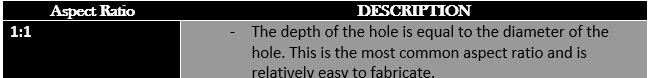
1:1| The dimension of depth is significantly greater than the dimension of diameter of the hole. If a fabric utilizes higher aspect ratio, it can be more difficult to craft and could be needing more advanced manufacturing methods. It is typical for them to find their application on high-density interconnect boards and therefore help compensate for the introduced complexity.
Via in pad and Advantages of VIP
Via-in-Pad (VIP) is a design method for printed circuit boards (PCBs) in which the vias are positioned contiguously the pads under the surface-mount sections of components. This technique offers several advantages:
- Space Saving: VIP allows for efficient and compact PCB which does not require solder mask openings around vias for routing of traces simultaneously and thus VIP is ideal for designs where available space is limited.
- Improved Thermal Management: Vias, locating under component pads contribute directly in the transmission of heat from components to the inner layers of the PCB, where it is difficult to reach, thus better thermal management is achieved.
- Reduced Via-Inductance: VIP has a lower inductance in vias than the old-style vias located off-pad. This leads to fewer issues regarding signal integrity, especially in high-speed designs.
- Enhanced Mechanical Stability: Adding connected vias in the edge of pads jointly with component increases component mechanical stability and thus eliminates mechanical stress and failure.
- Simplifies PCB Layout: Among all the benefits VIP provides in PCB, it is evident that the most remarkable is its minmization of the quantity of vias hitherto independent of routing area.
Generally speaking, VIP represents a viable method in PCB design whose purpose is to enhance the performance, reliability, and efficiency in the electronics devices of the present.
How to Make a Via in PCB layers?
To create a via in PCB layers, follow these general steps:
Design Stage
When choosing the places on the board, where vias are required to connect different layers of the board, at that time the phase of the PCB layout design can be used.
Via Placement
Vias placement is to be done with PCB design software in the arrangement of the desired locations. You can then select the size and type of via you require (in other words, through hole components, BLIND VIA, etc).
Via Size
Choose the size of the via communications dependant upon the characteristics of your target design such as the diameter of the openings and the dimensions of the pads that are to be connected.
Pad Design
Discard the pads which will be utilized with the via. The pads size – if large enough to accept the via and to guarantee a reliable signal line – should be taken into account.
Via Routing
Route traces are used in order to connect the areas on different layers of the PCB to the vias. Cross-connect the traces to the pads and vias accordingly.
Signal Integrity
Investigate the via concerns on signal integrity, particularly in regard with the high-speed designs of the circuit boards. By methods such as package via stitching or adding decoupling capacitors use to reduce signal interference.
Manufacturing process
Pre-manufacturing was also a crucial factor that you need to be considerate of. Make sure to choose a metal manufacturer that is capable of the pcb fabrication of your via design based on the design specifications like vias sizes.
What Kind of Via Should You Use?
The variation of vias’ use depends on many factors such as your PCB designing requirements, manufacturing facilities, and cost considerations. Here are some common types of vias such as buried holes and blind vias and their typical uses:
While selecting the type of via, various factors must be considered like the layout, your design requirement, the distance, signal strength, queasiness mandate, and also the capability for manufacturing. In addition, it will be better to contact with PCB manufacturer to decide the right kind of via that is for your designs.
What Size Should Vias Be?
Here is a table summarizing typical via sizes for different types of vias:
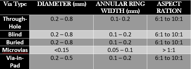
They are just examples, and if there are the special features of your PCB composition and PCB manufacture, you will have to substitute them with the correct ones of yourself. Such type of information is best found from your manufacturer or the design websites of the company since you may get details as accurate as possible.
FAQS
Conclusion
In the end, the via is the key element of the PCB design because it helps to create complex layout circuit and an efficient one. When we say via this is a small drilled hole vias that will goes through it into two or more adjacent layers or only two adjacent layers. As well as it will also allows the signals also the power just to travel between its layers. These copper tracks carry the signals from one PCB layer to another, preserve signal integrity, remove the heat produced during the operation of components and provide mechanical support for the components on the PCB. Thermal vias, placed in direct contact with the active components. multilayer board, the internal plating of a buried via must necessarily be completed before applying the two outermost layers to the that have high density interconnect board. The choice of trade such as vias and selecting the appropriate one according to a distributed design are the indicative sign of success of the function of reliability or reliable pcb assembly, and performance of the electronic devices, pcb laminates and pcb space.


