Go under the hood of two-layer printed circuit boards (PCBs) and understand how they work with this detailed guide. From performance-critical design concepts to industrial pcb fabrication nuances, you will learn many ways to improve your 2 layer pcb, layout or layouts, address signal quality issues, grounding strategies and various thermal challenges. Acquire the essentials of 2-layer PCB design by following professional advice.
What is 2 Layer PCB?
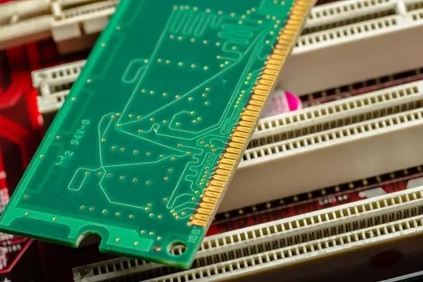
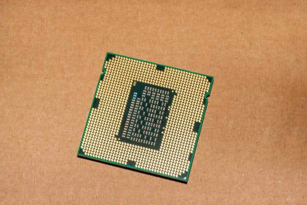
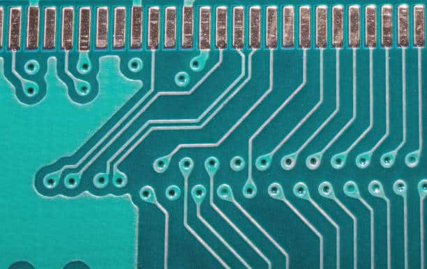
A 2-layer PCB, or double-sided PCB, is a type of a printed circuit board which is composed of two conductor copper layer, one layer lies on the top single sided boards and another on the bottom side of the board, whereas the substrate material (For example, FR-4, a dielectric constant related) is separated in between. Such layout is appropriate, being applicable in terms of different apparatuses because of its ability to adjust and costs. Regarding Double-Sided PCB, one can install all the components on one side and the traces can be routed on either side of the board. Also, they offer a way to use more choices of designs in complex circuits as compared to single-sided PCBs.
What are the key components and structure of a 2-layer pcb?
The composition and construction of 2-layer PCB does affect such performance and formula. Here’s a breakdown:
Substrate
Known as the PCB base material, also, it serves as the mechanical support and insulation among the conductor layers. Common substrates include fiberglass-reinforced epoxy (FR-4) in standard applications and polyimide in specialized ones.
Conductive Layers
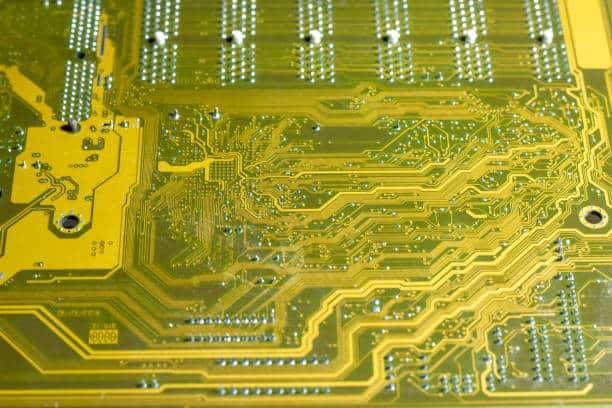
A 2-layer PCB is built on 2 conductive layers that are usually made of copper and they are laminated on both sides of the substrate. These layers provide the transport medium for the electrical signals, and this is how they are transmitted between the components.
Traces
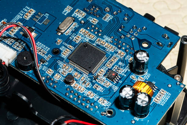
Characteristics of copper foil lines on conductive copper layers form these traces, allowing connections between components like resistors, capacitors, and integrated circuits. A trace may have electrical signals and power rails that go through the PCB.
Pads
Pads are the copper planes on the inner layer of the PCB surface to which the component leads are soldered or mounted. They are the provisions for the electric connections between components and the traces on the inner layer of the PCB.
Vias
Vias are minor drilling holes through the substrate linking the routing signals at different levels. Such interconnections can convey the signal change to the top and bottom layers and conductive inner layer and hence both the routing flexibility and reduced designs are achievable.
Silkscreen layer
The silk-screen layer is a non-conductive layer containing print-marks, labels and symbols printed on the circuit board (PCB) surface to indicate component location, polarity and other assembly information.
Solder Mask layer
Solder mask constitutes a protective layer that is applied over the otherwise conductive copper traces and pads for avoiding short circuiting and oxidation. It is typically made of green, blue or black coating material but some other colors are also used for the functional or aesthetic purposes.
What are the several steps of Manufacturing Process of 2-Layer PCBs?
The production process of 2-layer PCBs has multiple phases, which result in a double-sided PCB with the conductive copper trace on both sides. Here’s an overview of the process:
- Design: The process starts with the PCB design, using the computer-aided design (CAD) software. Component location, route size estimation, and layer connection creation are all part of the design.
- Substrate Preparation: A substrate material, which is typically fiberglass-reinforced epoxy lamination, is created. The substrate thus contributes in the part of mechanical support and insulation of the circuitry. The substrate often has a metallic layer of copper as thin as possible on both sides.
- Cleaning: The substrate is meticulously cleaned to remove any unwanted trace that may interfere with the production process.
- Photoengraving (Etching) for Layer 1: A photoresist layer etching process is laminated to one side of copper-coated substrate. The photoresist’s photographic image of the circuit pattern for the first layer is then exposed using the photomask and UV light. It is the photolithography process. The shielding of the areas not exposed to light comes from the photoresist. Once the PCB is suspended in an etchant solution the unwanted copper is washed away; only the protected copper remains resulting in the first layer of the conductive traces.
- Cleaning and Photoengraving (Etching) for Layer 2: The same is done for the top layer of the PCB. The photoresist is coated on the other side of a copper-clad substrate and the pattern for the second layer is transferred onto the photoresist through the help of photolithography. The PCB is then etched out to get rid of remaining copper which is no longer protected thus leaving behind conductive traces for the second level.
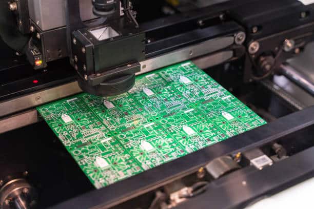
- Drilling: The PCB will have holes drilled through it which serves the purpose of accommodating through-hole components as well as providing vias for interconnecting the inner layer. Automated drilling machines are utilized in times when precision is being sought.
- Plating: A thin layer of copper electroplated on the fall of the drilled holes to strengthen them and interconnect the layers is applied.
- Solder Mask Application: Often, the layer of solder mask, usually green in color, is applied on both sides of the PCB. On the other side this blocks copper tracks and pads, so just soldering spots are exposed.
- Silkscreen Printing: The product name and other identifying information are printed on solder mask using a screen printing process.
- Surface Finish: Copper surfaces that are exposed must be protected by a surface finish and be easily solderable. Frequently applied surface treatments contain HASL (Hot Air Solder Leveling), ENIG (Electroless Nickel Immersion Gold), and OSP (Organic Solderability Preservatives).
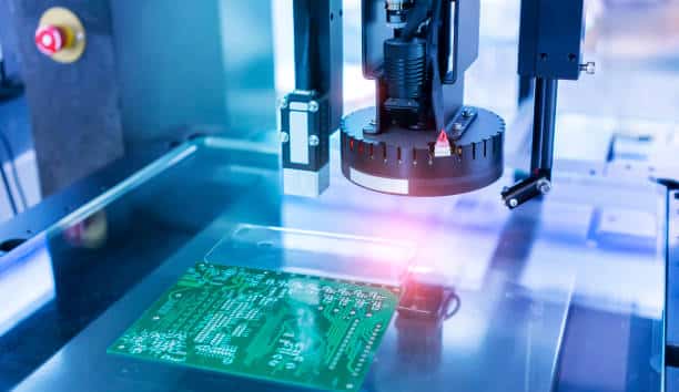
- Testing and Inspection: Once the PCBs are made, they go through the stage of electrical testing and visual inspection to see whether they comply with the standards of quality and specified requirements.
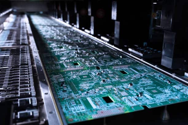
- Assembly: Following that, electronic components are soldered on top of the PCB with the aid of either automated equipment or by hand.
- Final Testing: Lastly, the final step is the testing of the built PCBs to assure their functionality and performance.
Through the double-sided process, which involves traces conductive on both sides, a PCB with increased routing flexibility and higher component density gets created as compared to that of single-sided PCBs.
What are the top and bottom layers of a double-layer pcb?
The same double sided circuit board-layer PCB or 2 layer pcb design defines the top and bottom layers as the two outermost layers of that double sided circuit board or boards in which mounting of components and predominantly routing traces lie. Here’s a breakdown of each:
- Top Layer: This is the highest layer (top layer), being the side that will be exposed when the PCB is assembled. The surface mount assembly (PCBA) is made of components mounted directly on the board which are connected together by routing traces. On the top layer most of the signal tracks and the important components such as the through-holes, resistors, and capacitors are placed, where they can be accessed and prototyped easily.
- Bottom Layer: The bottom layer means to the layer which comes at the bottom side when board is mounted. It features hardware parts that are installed on top of the circuit board as well as wires for the remote interconnection of the elements. This lower most layer (bottom layer) is often used for moving traces that couldn’t fit on the top layer or traces for distributing ground return and power connections.
Similarly, the top and bottom signal layers, of the PCB provide the fundamental connections two signal layers of the electrical and mechanical assembly that operate to activate the electronic component in its rightful place.
What is the purpose of copper layers in a double-layer pcb?
In a double-layer PCB or 2 layer pcb (Printed Circuit Board), two copper layer serves several important purposes:
- Conductivity: Copper is a superlative conductor of electrons. The curling copper material on a PCB is a path of electric current that runs through from one component to the other thus providing the correct functionality of the device.
- Routing: The copper foil with a pattern of traces that connect different components among themselves according to the production design is etched. Such traces literally connect the different components together in the way the current flows, conferring the circuit the ability to function.
- Ground and Power Planes: In a great many PCB designs, one or both of the copper layer sources are either allocated to the power delivery or the ground reference. Such planes being used, helps in minimizing noise, narrowing the signal quality and thereby stable power distribution throughout the circuit.
- Heat Dissipation: In addition, copper layer conducts the heat very well too. Copper’s ability to dissipate heat in the high power or high frequency circuit also help prevent components from overheating and ensures reliable working of these circuits.
- Component Mounting: Copper layer yields smears or pads or lands onto which the components are soldered. The role of these mounts is to offer both mechanical support and electrical connection to the components which will be in use.
Overall, the copper layer plays a key role in the proper operation of the double PCB layers by providing electrical connectivity, heat transferring, and mechanical support for the embedded components.
What are the Advantages and Limitations of 2-Layer PCBs?
Advantages:
- Cost-Effectiveness – In contrast to the more expensive multilayer PCB manufacturing, 2-layer PCBs are usually less expensive to fabricate; and as such they are ideal for budget-oriented projects or mass production.
- Simplicity – In turn, 2-layer PCBs being only two layers thick require less design and troubleshooting effort compared to more complicated multilayer configurations.
- Flexibility – In addition to their simplicity, 2-layer PCBs support design flexibility that can serve an extensive range of applications in which some circuit complexity and component density are allowed (moderate).
- Signal Integrity – Designed and fabricated 2-layers PCBs offer good signal strength because separation of signal and conductive material among the layers sufficiently lowers electromagnetic interference (EMI) and crosstalk.
Limitations:
- Limited Space for Routing – Offering only two layers for routing doesn’t give the density of trace space sufficient enough for components hence leading to unmanageable congested layouts and route challenges.
- Complexity Constraints – Though great enough for low complexity layouts, the 2 layer PCB may become insufficient for highly complex arrangements that need many signal layers and thorough routing.
- Signal Crosstalk – The crosstalk of signals originating from multiple layers on the board may still exist in the 2-layer structure even after all the precautions. This would especially affect densely packed boards.
- Conductive Material Separation – As in some cases, having a consistent distance between the conductive materials and the signal traces could prove hard leading to degradation of signal strength and to EMI performance.
What are the Design Considerations for a 2-Layer Printed circuit Board?
Designing a two-layer printed circuit board entails the thorough study of numerous factors which are key for high performance operation and production process. Here are some key design considerations:
- Layer Stackup – The stackup layer involves the number of two copper layers or more, dielectric material, and substrates in the PCB. Generally, a two-layer PCB uses a stackup that includes a top layer (signal layer) and a bottom layer (ground layer) or the power layer.
- Signal solidarity- Increasing signal solidarity is a key element for stable PCB functioning. A good signal routing procedure, which recommends a reduction of trace lengths, managing impedances, and signal crossing, prevents signal distortion, interference and ground bounce.
- Component Placement – A strategic placement that shortens the return path and makes the signal and minimizes the trace lengths of the components. Tuning in the components block by block and positioning the key ones in the priority order escalates the electrical performance of the whole system.
- Routing – Creation of the circuits in such a way, to reduce signal distortion, electromagnetic interference (EMI) and noise is a key factor. The signal traces should be made short, straight, and remote from additional high-frequency noise sources. In addition, signals running with high speeds must be guided with characteristic impedance that are controlled.
- Ground Plane – The use of a rigif ground plane on the bottom element of the antenna reduces the level of noise and impedance matching thus improving the low impedance return path or paths. Bringing together all the ground pins onto the ground plane avoids ground loops and provides a stable circuit.
- Power Distribution – Power distribution is routing the power traces so as to optimize their distribution on the circuit board and thus minimize the voltage drops and provide stable power supply to components. Decoupling capacitors situated nearby power pins affect the voltage and thus is responsible for filtering out noise and maintaining a stable voltage.
- Thermal Management – Efficient thermal management ensures temperature components are at maintainable levels for longer and more reliable performance. Thermal vias, heatsinks, and an airflow design can help the heat from being dissipated and prevent overheating of the devices.
- Manufacturing Constraints – Manufacturing restrictions involving minimum trace width, spacing and drill size should be considered to make sure that the PCB design is manufacturable within the accepted capabilities of the selected fabrication method. Follow design for manufacturability (DFM) standards to increase manufacturability and lower production costs.
- EMI/EMC Compliance – Implementing shielding techniques, filtering components, and reducing loop areas are the key points of EMI/EMC compliance. Thus, it reduces emissions, and the susceptibility of the device and reduces external interference.
- Testability – Test point inclusion and accessibility requirement for testing and debugging supporting their troubleshooting and quality assurance during PCB assembly and testing processes.
Through the incorporation of these elements in designing early circuits, engineers can have a two-layer PCB that fulfills the performance demands only early circuits, assures reliability, and eases fabrication.
What are the techniques in 2 layers pcb design of the signal Integrity and Noise Reduction?
Application of these methods will allow you to attenuate heat density as well as optimize the layout of 2-layer PCB in order to provide a device performance error-free and functioning at optimum condition. Signal quality and noise reduction these are probably the most important issues to consider while creating two thin layer two-level PCB designs. Here are some techniques to achieve these goals:
Ground Plane layer
Use high conductivity ground plane on the board as the return current path or reduce loop area on such conductors carrying noise.
Signal Traces
Trim the traces of the signal signals to the shortest possible while keeping them direct to ground signals enhance signal quality. Add annular traces for high-speed signals or controlled impedance to manage impedance and signal loss, inserting their width.
Separation of Signals
Decoupling high rate signal from the low-rate signal and cross them to suppress the crosstalk. Generate Shielding or Isolation for delicate Signals. Listen to the given audio and summarize the key ideas in your own words.
Decoupling Capacitors
Installing filters nearby the power pins of ICs will help against noise and a steady power supply would be maintained.
Impedance Matching
Make the wave’s impedance match the characteristic impedance of the transmission line to avoid reflections and deformations.
Routing and Layer Stackup
Walk through the wire routing ensuring that no route crosses over split planes or major components. To do so, we have the route components in stacked with more layers as to reduce the signal coupling and signal layers to increase signal immunity.
Use Differential Pairs
In the case of high-speed signals, it is important to work on signal quality and EMI reduction using differential pairs.
Grounding Techniques
Recognize the star grounding feature consisting of solid ground plane interconnecting all ground points to unique ones in order to reveal ground loops and noise.
What are the differences between 1 layer pcb, 2 layer pcb and 4 layer pcb?
The differences between 1-layer PCBs, 2-layer PCBs, and 4-layer PCBs lie primarily in their complexity, cost, and performance:
1-Layer PCB (Single-Sided PCB)
A 1-layer PCB or single sided pcb is a PCB made of only one layer or commonly known as the most basic pcb. A multilayer paper substrate (it is usually FR-4) on one side and metallic conductor (copper mostly) is located on the outside. The components and traces of a single sided board are all mounted on one side of the board, while on the other side the through-hole components are called leads, and you can pass them through holes and solder them to the pads on the other side by using a soldering iron. Rather that the more complex prints, PCBs that non have many components are simply used in the devices where the routing options and greatest complexity might not be the concern. Over the years, as the engineering became more advanced, renewable energy sources grew cheaper and easier to construct.
2-Layer PCB (Double-Sided PCB)
A 2-layer PCB or double sided boards consists of the co-joining of 2 conductive material layers through using the substrate as an interlinked medium. Plated through-holes (PTH) are normally used for connection of each layer. However, there might be PTH on the top and bottom side of the board and a connection is made that way. Consequently, multi-layer PCBs were targeted to intricate complicated circuits, that have high component density and they are also capable of doing more routing. In contrast, the double sided PCBs are built to support simple circuits. 2-layer PCBs or double sided circuit boards are widely applied for innumerous applications till these days in which it nicely combines the price and the performance factors.
4-Layer PCB
For a (4) four layer PCB or four layer pcbs,the substrate is four layers to thick and it can have a multi layer pcb in between the substrates. PCBs of this class and up have a lot more options in routing, are practically much denser in their components, can ship better signal quality, thus resulting in less electromagnetic interference prepreg layer is followed by inner layer 1. Ranging from everyday electronic equipment like phones, computers and digital systems working at high-speed they are the most widely employed. However, it would interesting to note that 4-layer PCBs not only are expensive than 1-layer and 2-layer types but also involve very intricate designs and complicated manufacturing processes that make them suitable where maximum performance and reliability are required.
Why 2-layer pcb is the most commonly used pcb than the other layered pcbs?
A dual-layer PCB, which is an equivalent for the most popular kind of PCBs in the world of the electronic circuits due to its flexibility and low cost, is the most widespread type of PCB. Boards of these kinds are good for people who want a board that does not give complex information but tidy and compliant information at once, so these circuit boards are used for different applications. Processing merchandise is simpler, requiring fewer stages as well as less materials and so manufacturing costs drop. The simplicity of EVs not only make them economical but also makes them easy to tauthen and tear apart as all their circuitry is lying open.
With their small layers, 2-layer PCBs easily fulfill the needs of lots of applications. This means, that these simple PCBs are well fitted for laying out a design with good signal integrity while still saving space. Although they may not represent the intricacies of the more complicated circuits and PCBs for the higher layer count (multilayer pcb), they certainly stand out at meeting the needs of these popular electronic components without additional complication or expenses whatsoever. Subsequently it allows them to substantiate their enormous implementation across a great variety of industries presenting them as a super essential and the most popular components of modern electronics.
Conclusion
Generally speaking, the double-track PCB enriches both ends of the electronic configurations with their durability and reliability. With its dual layer structure the new generation of PCBs provides a third signal layer, greater option for the digital signal, and power routing as well as wider opportunity to design circuits of higher complexity.
The upper and the bottom layers can provide vast space for components, hence, their mounting and interconnects are not complex. Both the surface-mounted and through-hole components can be handled with ease. This multi-functionality enables the creation of small designs with proper log-density for magnetics and power components as well as analog and digital sections. The solder mask layer and silk screen layers or more layers in addition let to the development of the reliability and manufacturability more which bring the precise soldering and improved maintenance.
With these things, the double sided circuit board or 2-sided PCB still form a base of modern electronics that underpin a variety of technology from consumer electronics to industrial automation and so on. Through the perfect combination of functionality, flexibility and cost-effectivness, they’ve kept already ensuring their relevance and wide adoption among the growing and rapidly developing surroundings of electronic engineering.


