Through Via In Pad (VIP) technology is an important facet of contemporary PCB design not only advantages they also pose challenges. VIP technology knowledge is a must-have requirement for engineers and designers to be able to design their pcbs for top performance, reliability, and manufacturing efficiency.
What is a Via in pad?
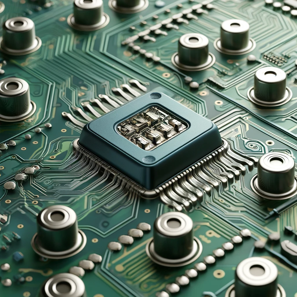
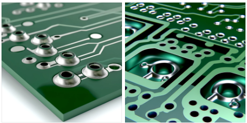
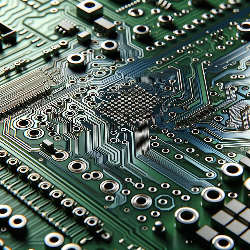
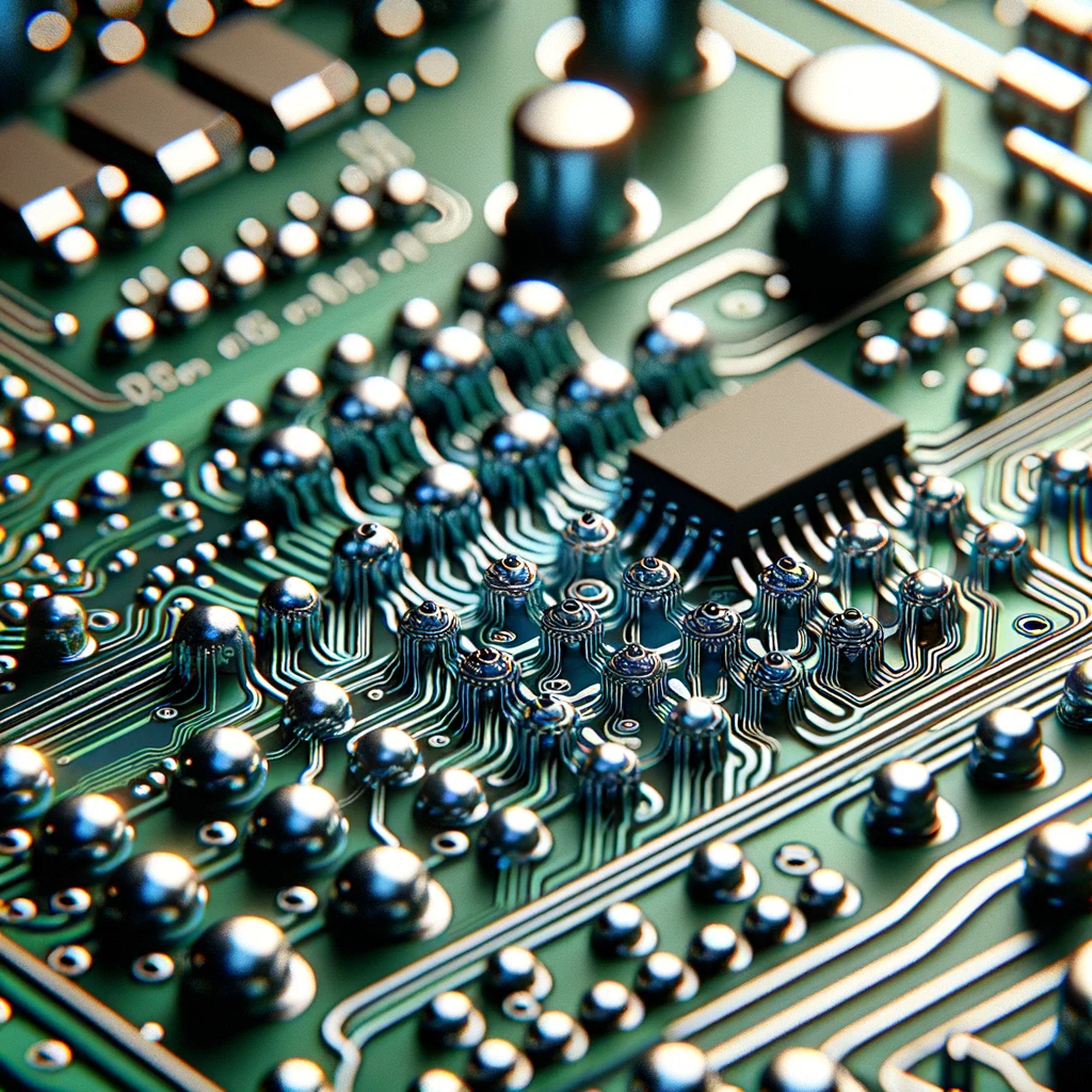
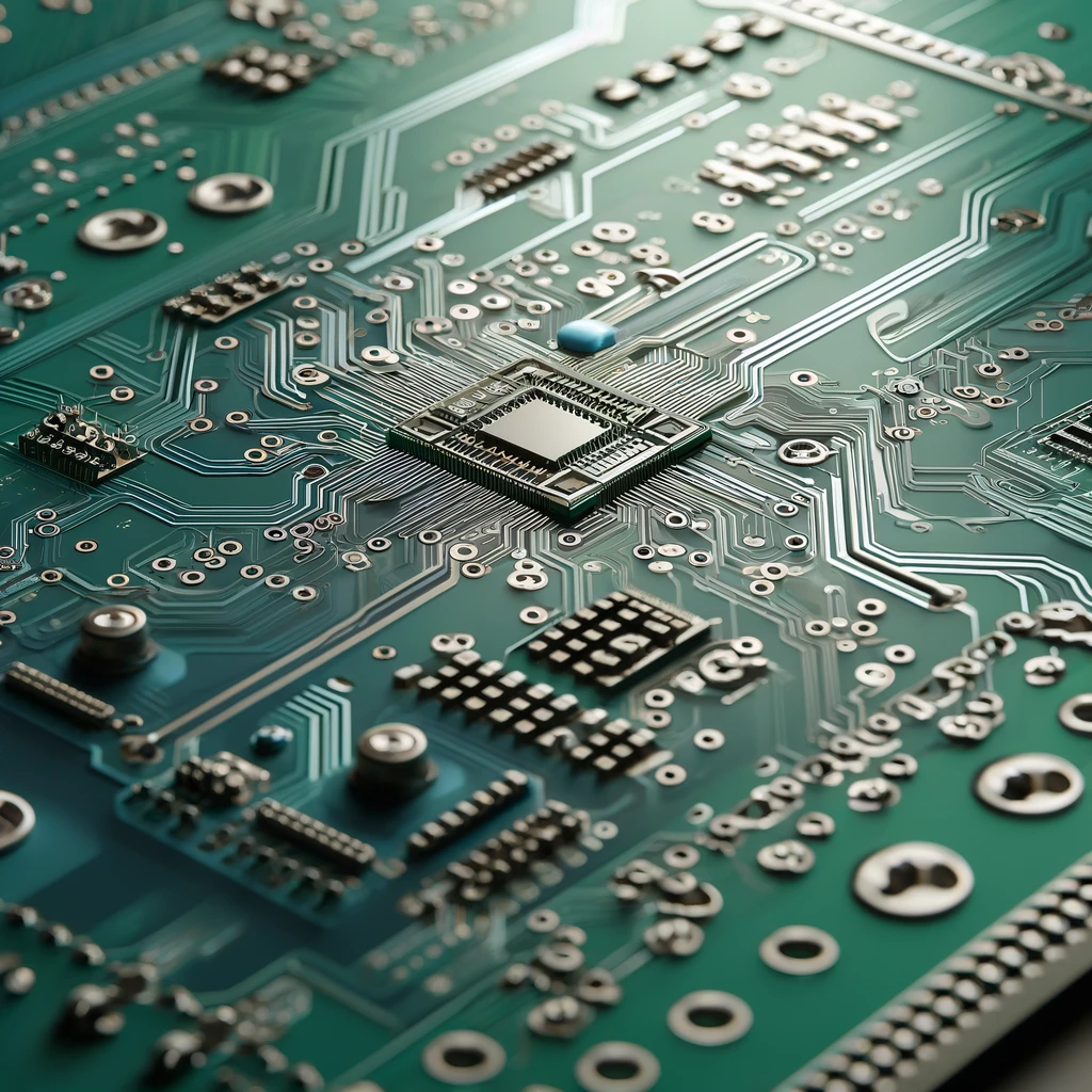
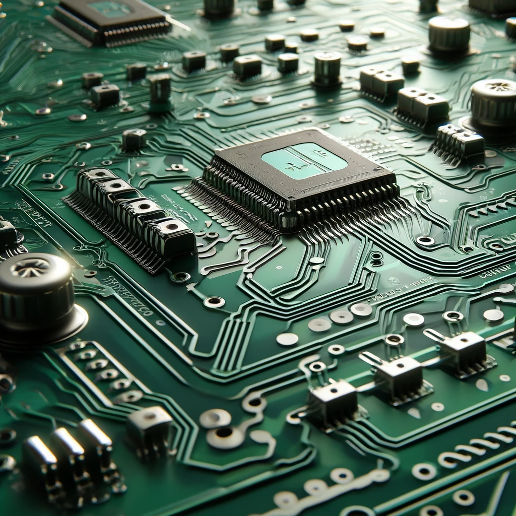
A via in pad (VIP) is a pcba design technique that is used in which a via is inserted directly in component pads, instead of being located at the pad’s sides. The process of the vias which are being typically filled with a non conductive epoxy, the capped and also plated over just to avoid or aware short circuit board or to avoid empty soldering which is caused it by a tin leakage. This leads to getting rid of the space, preserve the signals that define the uniformity and heat management in the electronic board.
When to Use Via-in-Pad in Design?

One of the prevalent technologies that use approach-in-pad (AIP) is typically seen in PCB design when some criteria or specifications necessitate that. Here are some situations when VIP may be advantageous:
- High-Speed Designs: VIP has the capability of being used in applications where signal integrity is crucial such as VIP, in high-speed PCBs designs. Incorporating vias leading directly to the contact points generates less signal distortion and, thereby, increases signal quality.
- Space Constraints: In case of confined PCB, VIP assumes close by abutment of vias with component pads, space for other components or routing is saved.
- Thermal Management: For example, elements that demand good heat dissipation feature VIP interconnections in connection with a copper plane and this aids in thermal management to the thermal pads.
- Signal Integrity: In designs, in which goes much signal integrity is the basic thing, for example, in high-frequency applications, VIP can be a tool that is able to minimize the signal losses and reflections.
- Routing Efficiency: VIP makes PCB routing clearer by letting designers travel with signal instead of standing apart from every signal which in turn becomes easier to route and it improves signal integrity.
- Cost Considerations: Although developing VIP technology contributes an additional processing step to PCB fabrication, VIP could simplify PCB manufacturing process or pcb fabrication process to pcb manufacturer, thus resulting in reduction of the layers and consequently cost savings.
VIP technology involves PCB layout to resolve integrality issues, including space limitation, thermal pad to thermal expansion to thermal vias as well as routing, that are depending of the purpose that PCB has for designing.
Benefits of Via in Pad Technology
Via-in-Pad (VIP) technology offers several benefits in PCB design:
- Improved Signal Integrity: Through the shortening of the signal tracks, VIP avoids signal distort and leads to an increasing of signal quality that is required for the high-speed circuits and the high-frequency ones.
- Space Saving: For instance, thin-line vias help in the direct routing of signals on the component pads which save the printed circuit board (PCB) real estate, in turn leading to compact and efficient designs.
- Enhanced Thermal Management: Via in Pad (VIP) makes the connector from pads of parts be provided by copper planes for enhancing heat dissipation and keeping the parts from excessively overheating.
- Streamlined Routing: VIP smoothen the complicated PCB routing process by facilitating the surge signals and reduces the signal path complexity.
What are the different types of vias?
Through-Hole Via in pad
A standard thru-hole plated incorporating via to traces on both the sides in through hole vias.
Blind Vias
A blind via is given to the outer layer of a PCB, and it goes to an inner layer or multiple inner layers or internal layers but does not completely penetrate through the board layers.
Buried Vias
Pathway that takes hops (via) between one layer or a series of layers in a PCB but it does not extend to the outer layers of the PCB.
Microvia
Nowadays a narrow hole usually under 0.15mm in diameter is targeted by “via” in HDI PCBs to create a higher density and to improve the signal transmission quality.
Filled Via in pad
By utilizing a via made of conductive or non-conductive material to aid in reliability and thermal conductivity, this approach can also mitigate resistance, a critical electronic components factor in device efficiency.
What are the advantages and limitations of via in pad routing?
Advantages
- The increase of signal integrity in shorter paths of signal.
- In space, the number of components usually needs to be reduced and thus PCBs are designed to save as much physical space as possible.
- Encouraged thermal conductivity, which helps thermal dissipation. Wrap
- Simplified routing, minimizing signal path complexity, thus, reducing the number of the components required in the circuit.
Limitations
- It is attributable to both rising manufacturing complexity as well as higher cost.
- For example, a intricacy of soldering or solder paste, which can create problems if not control to prevent errors.
- Possibility of reliability problems if be not manufactured or designed someone stylishly.
- Setting limit to functional aspects that can create issue with signal integrity and so has to make the planning carefully.
What are the differences between conventional vias PCB design and via in pad Printed circuit board design?
Conventional PCB Design:
- Vias are shifted apart from the pad of the component. This prevents any traces from moving towards the pads by chance.
- Demands extended space on the Printed circuit boards.
- Shorter signal length appears to cause signal debasing.
- The longer the interconnection paths are, the more complex the routing (due to longer connections).
Via in Pad PCB Design:
- Vias are integrated into the layer on the same pads as where the component pad are solder mask.
- The component is reduced in pad size and thus more space can be utilized on the circuit board, leading to a more mobile and compact design practice
- Short paths indicated on signals, that enhances signal integrity.
- Simplify routing; complex signal components are least useful.
FAQS
How does VIP technology compare to conventional PCB design?
The VIA used in VIP technology is different from vias used in conventional PCB designs; VIA in pad design are placed directly at components pads and it leads to shortening the route between close pads and to personal routing and space savings.
How does VIP technology impact signal integrity?
VIP can lower the effects of signal distortion values by minimizing signal paths and using easy to trace routes. VIP is especially effective in high speed, high frequency applications.
What are the challenges of using VIP technology?
The product VIP technology manufacturing encounters challenges such as soldering and reliability, at the same time, design is very much restricted. Usually, VIP is dubbed as the most complex technology in manufacturing either increased manufacturing complexity.
When should VIP technology be used in PCB design?
VIP technology is commonly applied when speed of transmission is critical or where space is a limited resource or thermal management or routing efficiency are concerns.
Conclusion
In the end, VIP technology is the key to the successful design of PCBs and there are numerous advantages, which include, excellent signal integrity, small size saving space required, effective thermal conductivity and more simple routing. In fact, it is acceptable to place vias in SMD pads, but there are certain myths about when and how to place these vias Be that as it may, VIP innovations have some of their own problems, namely the manufacturing complications, the soldering difficulties, and the design restrictions and then The manufacturer will have to eliminate surface bumps.
The process of the vias which are being typically filled with a non conductive epoxy, the capped and also plated over just to avoid or aware short circuit board or to avoid empty soldering which is caused it by a tin leakage. However, it will also prevent solder from wicking and solder joints to solder balls. Such issues, however, can be dealt with when all relevant measures are followed. Broadly, VIP technology is the right tool for designers intending to achieve the best performance, dependability and productivity more for the circuitry, particularly in cases of high speeds and high frequencies or high density pcb designs and using pcb design tool. With via in pad, the drill hole for the via is inside the pad. This means you can not tent the via with soldermask.


