To design PCBs correctly when dealing with traces, you should be well aware that trace width and current are in close relationship. This knowledge is important, for without it, there is no guarantee that this PCB will be at its best and remain strong under all kinds of conditions. In this article, we will be looking specifically at trace width, why it matters, how it impacts current handling capacity, and tips to get better mounting performance out of your PCB.
Understanding PCB Trace Width and Current

Token width implies the width of conductive courses or tracks on a PCB. Repairing this type of damage requires replacing the small amounts of connecting traces that are damaged with electrical signals. The current is the flow of electrons through these lines, but being small, they do not block light. The trace width and current relationship is vital because the PCB board’s capacity to handle its load of electrical supply won’t be disrupted or damaged in such a way that it will overheat or create problems with it.
Factors Influencing Trace Width and Current Relationship
The trace width and current relationship in PCBs is influenced by several factors:
- Current Carrying Capacity: A broader track can be made more bulky but more prone to overheating.
- Temperature Rise: This is an impact that might be caused by the high temperature which can destroy the working circuit.
- Copper Thickness: Copper trace layer with the largest thickness is then preferable as it offers better conductivity and higher current.
- Trace Length: Speaking of traces, the longer they are, the more they act like official resisters and can even generate some heat.
- Ambient Temperature: The thermodynamic performance of the structure decrements due to high temperature surrounding it and then there is a heat dissipation. So the structure is not able to thermalize.
- Layer Placement: Outward heat loss dissipates faster than the inner area radiated surface.
- Conductor Surface Finish: The surfaces of the coolant around the engine are rough and lead the flow in the direction of the combustion chambers. This causes the coolant to be heated to very high temperatures.
- Thermal Pathways: Surface mount items, including thermal vias and heat sinks, can provide a means of more effective temperature sag.
In building traces a designer must consider the following factors: current, heat, and chance of damage that eventually will burn.
Importance of a PCB Trace width calculator
Here’s a table of a PCB trace width calculator, along with the typical formula used for calculating trace width:
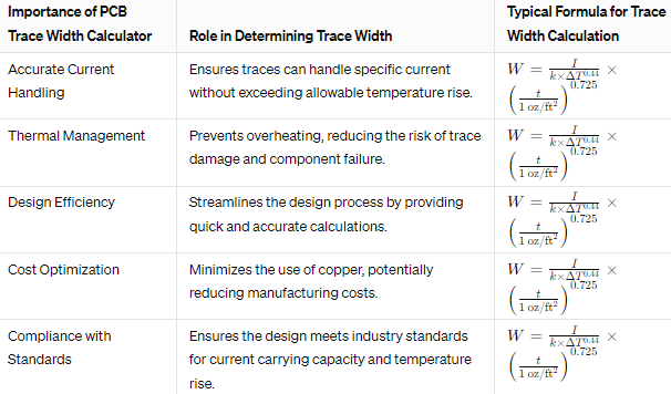
In the formula:
- W is the line width after the outer and inner materials are affixed, measured in mils, or mm.
- I is the immediate distance between the two poles (in ampere units).
- k is a constant that is derived empirically, with door and side wall intensities that are close to 1.0 in the internal layers and close to 0.8 in external layers.
- ΔT is the tolerable temperature change (in °C), which determines our capacity for cooling.
- This is an amount of copper that should be used for making one square foot, which is 1 oz/ft2, or 35 micrometers (35 µm).
The formula based on this notion is the starting point for finding the trace width and other values, but you should keep in mind that the exact constants and exponents can be different from the literature and may vary depending on the trace width and layer count to minimum trace width.
Current to temperature rise
The correlation between price current and temperature increase in a printed circuit board license is inspired by the fact that the current flowing along the trace generates heat due to the given resistance or resistivity temperature coefficient. The key factors affecting this relationship include:
- Resistance: As the load on the trace increases, the generated heat becomes too high for the safe operation of the device.
- Current: The heating process has a positive correlation with I2R heating radiation that is proportional to the current.
- Thermal Conductivity: The heat dissipation is enhanced by materials with high conductivity, which, as a result, will decrease the temperature rise.
- Ambient Temperature: The temperatures of the surrounding area that I live in determine the beginning point of surface rise.
- Surface Area: Larger and wider window panes offer a greater surface area for heat dissipation, thus reducing temperature increases.
In other words, trace’s exclusive temperature rise always comes with higher current and resistance, but it will be reduced by better heat dissipation and cooling and in a low ambient environment.
PCB Trace Width vs. Current Table
Here’s a comparison table showing typical PCB trace widths for various current levels based on different copper thicknesses and a 10°C temperature rise (values are approximate and for illustrative purposes only):
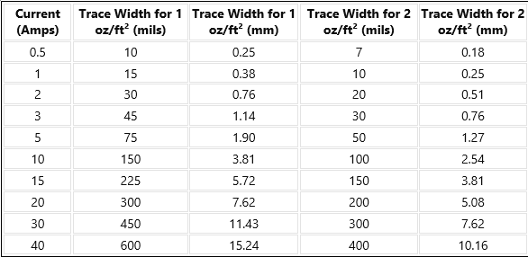
NOTE: This table visualizes that the lower trace width with growing copper thickness is for the same current level. This is the result of the increased current-carrying ability of thicker touch layers. Bear in mind that in reality, these values are only guidelines and may be influenced by the particular design requirements, the rated temperature rise, and other parameters. To prevent similar issues in the future, always refer to the IPC-2152 or use a PCB trace width calculator for even greater accuracy and design parameter functions tailored to your specific design parameters.
What is a PCB trace width calculator?
With a PCB trace width calculator, PCB designers are helped to calculate the suitable trace width for the conductor, which is based on the current required for the conductors and also on other factors like the rise in temperature and copper thickness. This brings about the harmonious condition that a sufficient current can be maintained without the traces overheating or bringing out other issues.
The calculator typically takes into account factors such as:
- The total amount of current that the trace should wisely supply.
- With an acceptable temperature rise above the current level of the chase.
- The thickness of the copper layer is called the loss of the conductor.
- The temperature is ambient.
- By considering such factors, the calculator utilises the formulas derived from specifications like IPC-2152 to compute the most suitable trace width for carrying the required current safely.
Here’s a simplified graph that illustrates the relationship between trace width, current carrying capacity, and temperature rise:
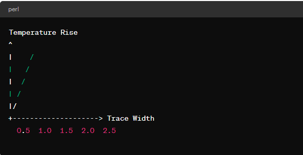
In that graph above,
- With the trace width measured along the X-axis in millimeters (mm),.
- The vertical y-axis marked a temperature increase in ºC.
- The gradient of the line reflects that as the trace width increases, the temperature rise due to the same level of current diminishes.
The array shown here is only a demo of real graphs that are used in PCB trace calculators, which account for factors like copper thickness and trace length, among others.
Calculating Optimal Trace Width
Determining an optimal trace width on a PCB requires delving into multiple issues like current-carrying capacity, temperature rise, copper thickness, and environmental temperature. Here’s a general approach to calculating optimal trace width:
- Determine the Maximum Current: Identify the essential maximum current that the diagnostic is going to carry in your circuit.
- Choose the Acceptable Temperature Rise: Establish the threshold temperature for the trail, the safest level at which the trail can function. For instance, choose 10 °C, 20 °C, or 30 °C, as required by your operations or by the material canning your PCB.
- Select the Copper Thickness: You are required to choose a copper layer for your PCB board. The standard thicknesses are (35 µm) and (70 µm). There are other thicknesses, though, that you can choose from.
Use a Trace Width Calculator or Formula: Teach the PCB trace width calculator about the maximum current, and maximum desired temperature rise the operating temperature rise, and the copper thickness. Alternatively, you can model the parameters using a formula from the IPC-2221 standard. A commonly used formula for external layers is:
where:
- W is the size of the wire in mils, where 1 mil is equivalent to 0.001 inches.
- k is a constant that depends on copper’s thickness (for 1 oz/ft² copper, this average is around 0.725).
- significant for I is the electric current in amperes.
- ΔT is the increase in temperature in °C.
- Adjust for Specific Conditions: Besides the routing capacitance, you should also make provision for the involvement of proximity to heat sources, the usage of thermal vias, and the desire for impedance matching in top-speed designs.
- Validate the Design: The last step is to check the trace width either by simulating or using a test, especially when utilizing high current or high frequency in the critical application.
High-current PCB layout guidelines
Keeping in mind the fact that PCBs will be used in high-current applications, the designer should follow the rules to produce a reliable and safe PCB. Here are some key points to consider:
- Trace Width: Enlarge the conductors value, which will have high currents to reduce the resistance and thus the heat generated. With the aid of a trace width calculator, figure out at which trace width you should set up the system so the required current flows through it.
- Copper Thickness: Use a thick copper wire (like 2 oz/ft2 or higher) to serve higher currents without getting hotter.
- Thermal Management: Design the circuit board carrying heat sinks, thermal vias, and any other mechanism that would dissipate the heat most efficiently.
- Short Paths: In order to optimize current flow, take the shortest and straightest path only to limit resistance as well as determining voltage drop.
- Multiple Layers: Take advantage of various levels and generate alternative routes through which heat can escape.
- Component Placement: Arrange the high-current parts near each other and power sources to minimize cable lengths.
- Via Sizing: Engage bigger vias or several parallel vias for carrying large current in order to get sufficient conductivity.
- Clearance: Make sure that you leave enough active space between the high-current traces and other traces or components to avoid arcing or short circuits.
- Isolation: identify the sensitive signal lines from the high-current paths where interference should not exist.
- Testing: Perform adequate testing, including the thermal analysis, to ensure that the PCB remains stable after being exposed to the current maximum that is expected of it.
Complying with these rules, you can come up with a PCB that needs field currents to be processed safely and efficiently.
Max Current, Determining Trace Temperature, and Resistance Calculation.
Table 1 is developed to ascertain the amount of plus current, trace resistance, and temperature with the assistance of different parameters, i.e., determining trace thickness, width, and ambient temperature. For simplicity, I’ll present one example that shares common values. As a rough number, these are sentences, and exact counting might be done with some special materials and conditions.
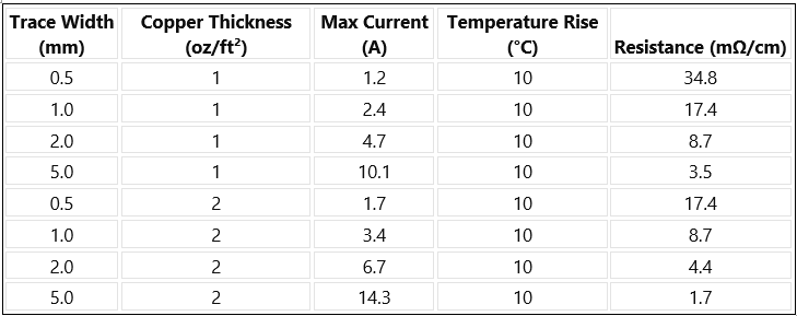
Note:
- The maximum current values are built on the ohmic values under the IPC-2152 standards, which are 10°C higher than the ambient temperature (25°C).
- These response values are approximate and were obtained using a room-temperature copper weight resistive of 1.72 x 10^-6 Ω·m. The real resistance can be affected by numerous factors and can also vary according to a specific material and condition.
To get more precise and definite outcomes, it is recommended to use a trace-width PCB calculator and refer to IPC-2152 standards.
Resistance Calculation
The resistance of a PCB trace can be calculated using the formula:
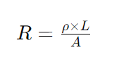
Where:
- R is the resistivity in ohms (Ω).
- ρ Gravity is related to the resistivity of the material (for copper, at room temperature, it’s nearly 1.68 x 10⁻⁸−8 Ω·m).
- L is the actual length of the trace converted from meters (m).
- A stands for the cross-sectional area of the flow and is measured in square meters (m2).
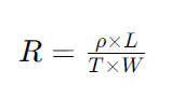
The trace cross-sectional area A can be calculated as follows:
- A=T×W
Where:
- T is the dynamic variable that measures the thickness of the trace in meters every time it is varying (m). For example, 0.035 mm/ft2 thickness is equivalent to 1 oz/ft2 and 3.5 x 10⁻⁵−5 mm/ft2 is approximately equal to 3.5 x 10⁻⁵−5 m.
- W is the signal track width in meters (m).
So, the resistance calculation formula becomes:
For example, let’s calculate the resistance of a PCB trace that is 5 cm long (0.05 m), 1 mm wide (0.001 m), and has a thickness of 1 oz/ft2 (approximately 0.035 mm or 3.5 x 10⁻⁵−5 m):
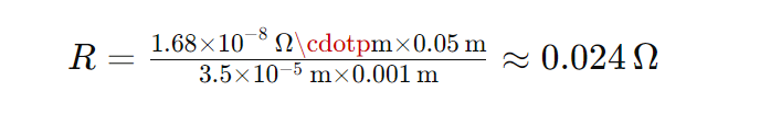
Therefore, the resistance of this trace will be around 0.024 ohms.
Voltage Drop Calculation and Power Dissipation Calculation
To calculate the voltage drop and power dissipation for a PCB trace, we can use the following formulas:
Voltage drop
Where:
- I It is the current that travels through the path in amperes (A).
- R stands for the resistance of the trace, measured in ohms (Ω).
- Power Dissipation (P):
Here’s an example table with some sample values for a PCB default trace width with a resistance of 0.024 Ω (as calculated in the previous example):
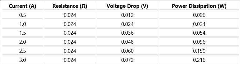
In this table:
- Voltage drop can be calculated by multiplying current by the resistance (e.g., in the case of 0.5 A voltage consumption, drop dropped=0.5×0.024=0.012V).
- When taking the Power Loss column or Power Dissipation, this is derived by multiplying the voltage drop by the current (e.g., for 0.5 A:=0.012×0.5=0.006P=0.012×0.5=0.006 W).
These estimations are key to ensuring that the PCB trace thickness calculators can manage the expected current without unnecessary voltage drop and excess heat accumulation due to power dissipation.
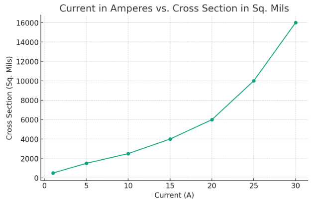
Below is a graph showing the relationship between A/amps (current) and CSA/mil (cross-section area) of a commonly used copper conductor. In line with the increase in the current, the operator must satisfy the demand through the increased value in square meters to safely pass the current without overheating to the external trace layers.
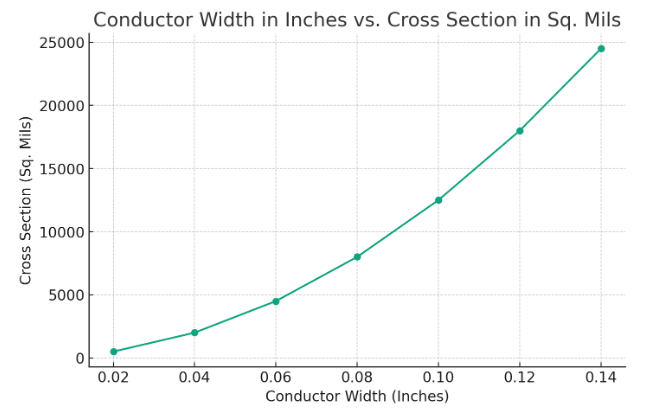
The graphic below shows the relationship between conductor width per inch and cross-section per square mill for a standard copper conductor. The width of the conductor has a direct effect on the cross-sectional area in square meters. The area of the conductor increases as its width increases, allowing it to handle more current and deliver more power levels.
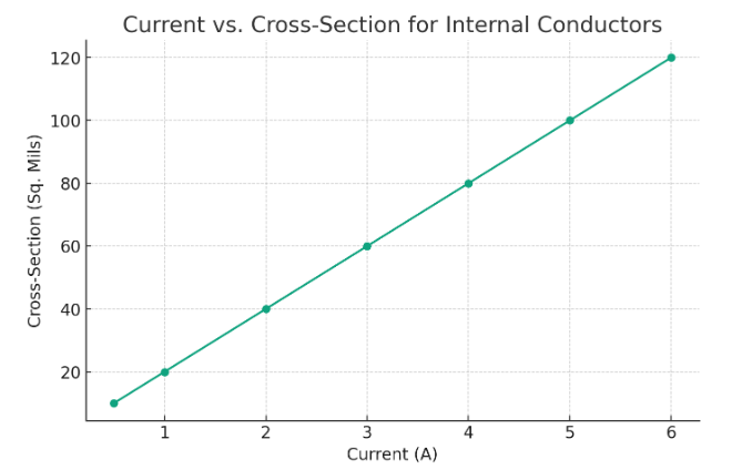
As the current increases, the required cross-sectional area to carry the current grows proportionately to the increase in current to prevent overheating. Unlike the external traces conductors, internal conductors to internal trace widths have to be ‘deeper’ and wider since overall heat dissipation from the layers of the printed circuit boards is more limited.
Current carrying capacity for 2 oz. copper thickness with a temperature rise of 10 degree Celsius
Here’s a table showing the current carrying capacity for a 2 oz. copper thickness to copper traces with a temperature rise of 10°C, based on IPC-2152 standards:
Trace width (mm)
- 0.5
- 1.0
- 2.0
- 5.0
- 10.0
- 15.0
- 20.0
Current Carrying Capacity (A)
- 2.6
- 4.2
- 6.8
- 12.2
- 20.4
- 27.2
- 33.1
The table shows the current carrying capacity for the specified electric motor design parameters as well as the variation in actual current capacity due to particular design and environmental factors. IPC-2152 standards are to be followed for accuracy, or a PCB Internal traces width calculator is better to be used to calculate trace width.
Conclusion
Trace width and current are closely related, so more awareness of the relationship helps to design working and accurate PCBs. By adhering to all the necessities that contribute to this relationship and being diligent about the principles of best practices, you will ensure the continuity of this PCB application for a long period of time.


