The soldermask has a significant impact on the safe operation of PCBs, wiping out short circuits and environmental factors. Discover the significance of solder mask and PCB blocking and the way they are used in electronics making.
What is a Solder Mask?
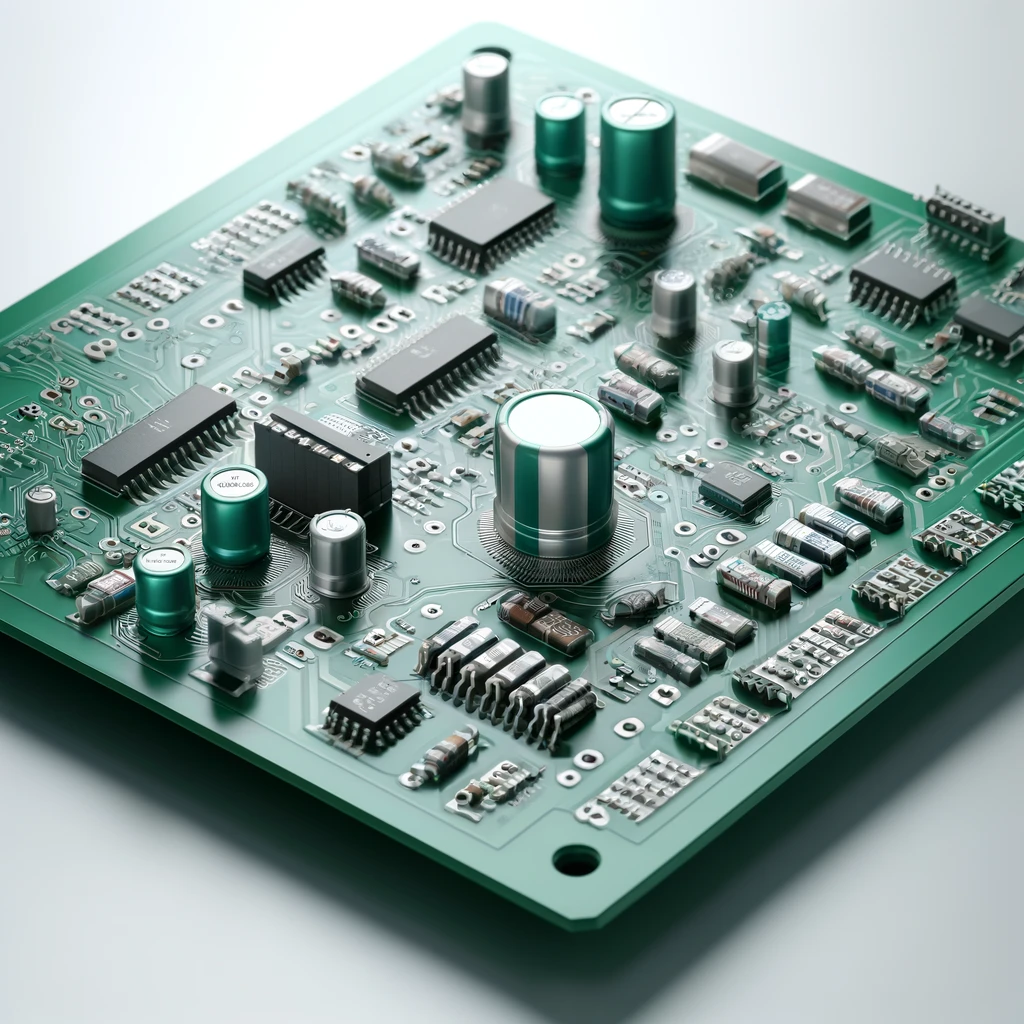
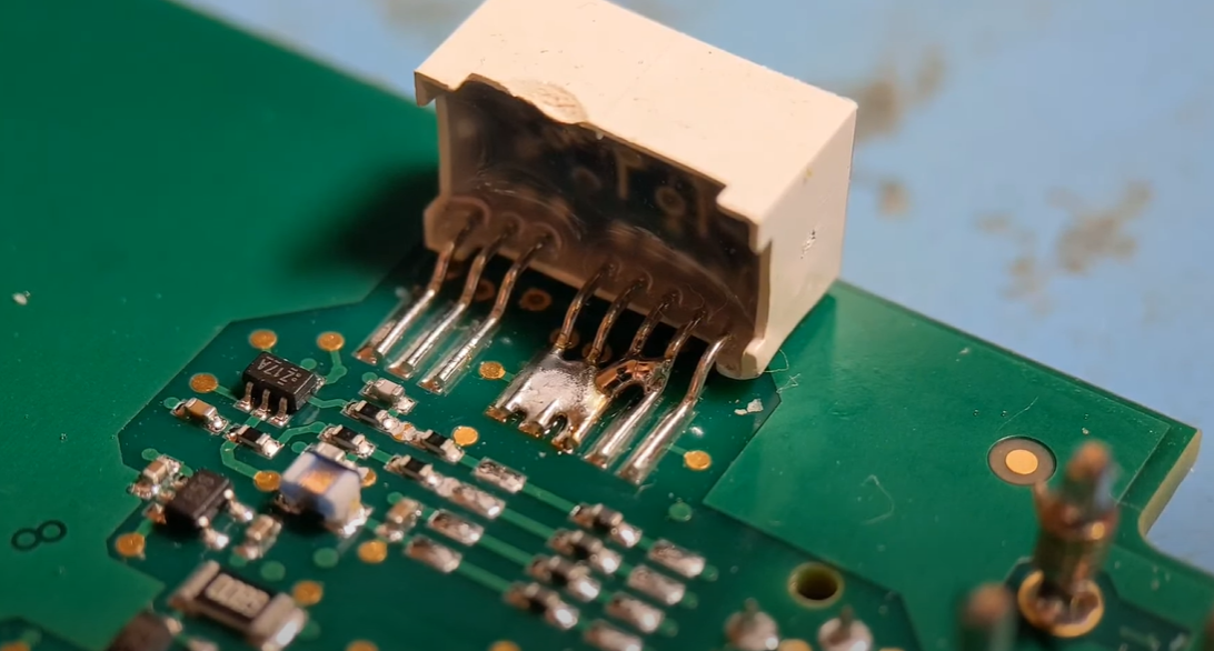
Solder mask is frequently used as a shield to prevent the molten solder from bridging and shorting the closely placed solder pads component pins that are present on printed circuit boards. The typical maler consists of heat-resistant polymers resin that adheres well to the PCB surface. The Key features of solder masks include:
- Insulation: Solder resist, which is coated on PCB, prevents the unintentional jump between the conductive lines.
- Protection: It acts as a barrier screen for the exposed metal tracks from diverse environmental aspects like moisture, dust, and chemicals that might be dangerous to the system of tracks.
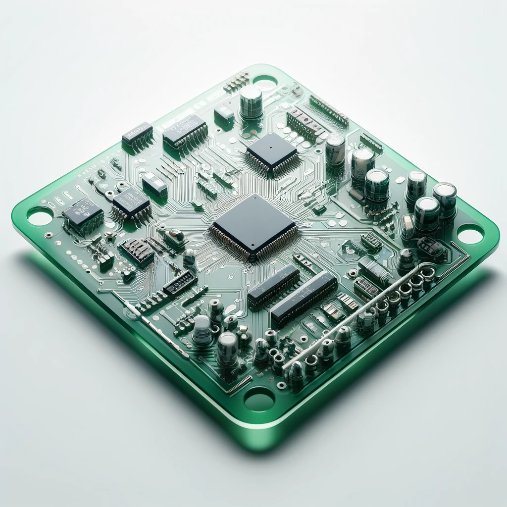
- Identification: Solder masks can be varied in colors (commonly green but can be other colors like red, blue, and black, for example), so assistance in assembly and component recognition is much easier.
- Alignment: The various produced solder resist features ease the process of placing components accurately on the solder in the PCB assembly process, thus reducing the possibility of assembly process misalignment errors developing.
- Solderability: The solder mask resists the solder components from sticking to its surface but does not bond weakly to the area exposed, which guarantees the soldering joints to be robust.
The solder mask layer is one among others that protects heat-sensitive components and forms a barrier against an external world. It shields circuit designs from potential hazards and guarantees their functionality.
What Is the Significance of Solder Masks in Electronics?
The significance of solder masks in electronics is paramount due to several reasons:
- Prevention of Short Circuits: The solder mask acts as a guard against electrical contact between conductive PCB traces (PCB) and unintentional circuit shortcuts.
- Insulation: The buildup of solder masks around conducting traces is a protective method that enables the flow of current only through the specified paths, reducing interference and product anomalies.
- Protection from Environmental Factors: Solder resist protects the traces that are left exposed to the agents of destruction, such as moisture, dirt, chemicals, and so on. These causes would be corrosion, oxidation, or other kinds of degradation without using this source, leading to circuit failure.
- Improved Reliability: It not only increases the confidence that there will be no short-circuit incidents, but it also contributes to the overall protection of electronic devices against the elements. Beyond this, solder resistance also makes the devices more reliable and durable.
- Facilitates Assembly: The history of solder resist adds up to working in a line during the assembly process with visual guidance and alignment markers. Contrary to conventional equipment, which leaves room for alignment failures during the soldering process, the integration of components into printed circuit boards increases the accuracy of the placement, therefore minimizing the possibility of component misalignment.
- Enhanced Solderability: In contrast with the solder mask that disallows solder from going through it, it is still possible for the solder to bond at all the revealed points so as to form strong and robust solder joints.
- Identification and Branding: The pasty solder mask is most often made with green, but other colors like red, blue, and black were also used. The label also pinpoints the tasks that workers are required to do in addition to contributing to the brand image of the manufacturer.
Overall, the main task of the solder mask is to determine if the temporary solder mask resists and adds to its reliability. To a great extent, this is the key to the performance and long-lasting electronic circuits of the device.
How is a solder mask applied to a printed circuit board (PCB)?
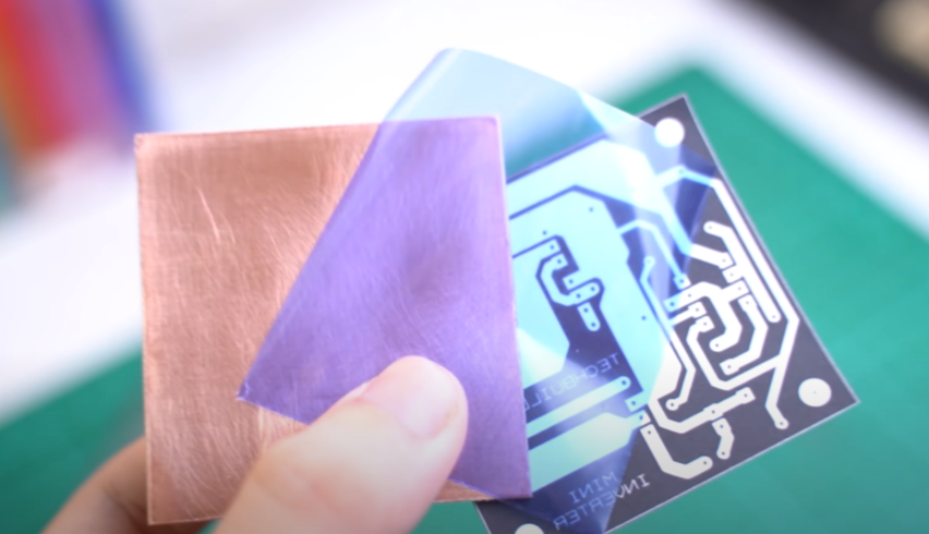
Surface Preparation the PCB surface is totally cleaned, and the prepared layer is used for the solder liquid masking tape material for the best adhesion to happen. This process involves the cleaning of any contaminants from the area of copper traces or copper and silkscreen layers, including fusion or oxidation marks.
Application of Solder Mask Material
The solder resist material, usually a liquid epoxy-based polymer, is applied to the surface of the PCB using one of several methods:
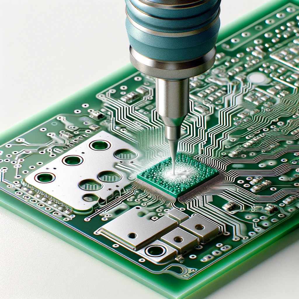
Screen printing: While it may represent the majority of solder mask applications that are performed, this is the most common method. After the pattern is in place, a stencil or mask is created, respectively, full of openings corresponding to the areas of interest and willing to be solder masked. The stencil, which has already been filled with the solder resist material, is used to cover the entire surface of the PCB through the openings in the stencil by using the squeegee or roller.
Spray Coating: In this method, the solder resist material is played out on the surface of the PCB using the equipped tools. Spray is sprayed in order to reach all of the suspended components.
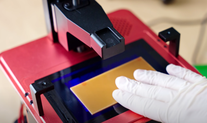
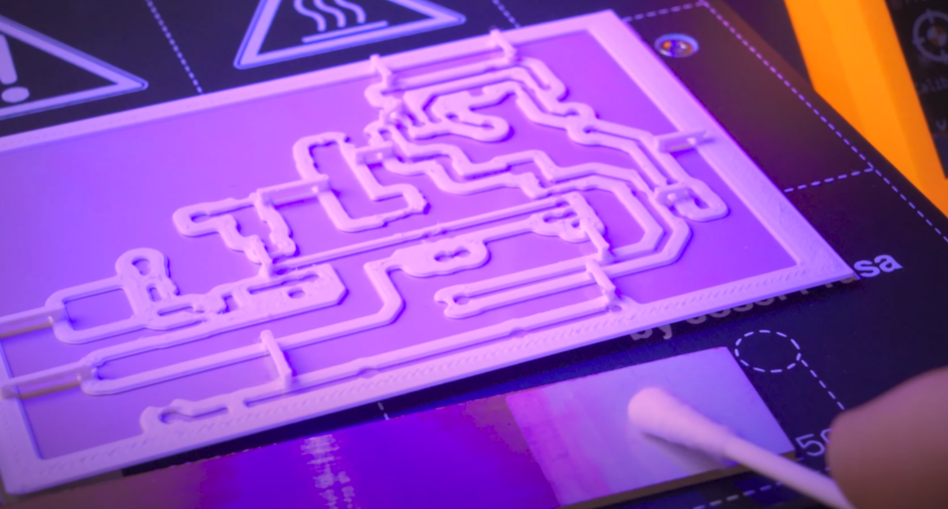
Photo Imaging: The first technique or method is known as dry film solder masking. The application of the material that is made into a film is done on the surface of the PCB. An overlapping pattern of the desired solder mask is then transferred to the dry film from the picture using a picture-sensitive process. Through the introductory process of washing unexposed regions of the film away, ultraviolet light can resemble the pattern of the solder mask left.
Curing: Thereafter, upon applying the solder mask to the PCB, it is cured to bring back the hardest protective layer. Heating by placing the PCB peelable mask in a convection oven at elevated temperatures is usually the way to go. Thermal curing can be applied to all materials that include an infusion of ultraviolet light for photo imageable solder mask materials.
Inspection and Touch-Up: The cured PCB is then inspected to be sure that the solder mask is properly applied and that there are no defects, in addition to the pinholes or lacking areas of coverage. Air bubbles could be used to apply a temporary solder mask, which will be fixed during further periods of the PCB manufacturing process.
What are the different types of soldermasks?
In the electronics field, there are multiple types of soldering mask materials, and the effects and application of each type are different depending on its characteristics. The most common types include:
1. Liquid Photo imageable Solder Mask (LPSM):
- The organic solder mask type is used for covering the surfaces after being applied as a liquid and cured using UV light exposure.
- It gives great resolution and classical SMT (surface-mount technology) for fine-pitch applications.
- LPSM is a widely used technique for implementing high-density PCBs, which demand higher precision for the alignment and feature areas.
2. Dry Film Solder Mask
- It is of the dry film solder mask type, which is a flexible polymer film covered with a photosensitive material.
- It is spread out over the PCB surface, and after being exposed to LED lights through a mask, the photo allows one to view the needed layout.
- Next, the residue of photoresists is removed to leave the solder mask, then the exposure area.
- However, dry film solder masks are widely known for their oligophobicity as well as their superb abilities in covering the mask dams.
3. Thermal Cure Solder Mask
- Via the thermal method, solder mask liquid goes through curing in a curing oven after it is heated to a certain temperature.
- This kind of solder mask provides not only good adhesion but is also a fairly recognized material. It means it is suitable for a lot of applications.
- Here, many times, it is utilized in elevated-temperature situations and also for applications where better pliability is required.
4. Pastes and Inks:
- Solder mask pastes and inks get used where there is a need for a selective coating or where touch-ups might be required.
- They are applied to products with the help of a dispensing device or screen printer.
- Solder mask pastes and inks provide added flexibility and are commonly used for the small-size repair of minor faults or the application of an additional protective layer to specific zones of the PCB.
5. Conformal Coatings:
- Though not completely true with this solder mask definition, conformal coatings serve along this line by adding a protective shield across the PCB as a whole.
- Conformal coatings are used after soldering and also after components are placed, which are the best safeguards against moisture and other pollutants that might exist in the ambient environment.
- Spraying, dipping, or brushing can also be used for the application process. Create an interactive learning environment by employing various strategies for teaching in-demand careers. Students should acquire knowledge through both theoretical and hands-on experiences. Enhance learning through practical and relevant lessons that showcase the relevance of their education to their future careers.
How Does a Liquid Photoimageable Solder Mask Work in Electronics?
A photoimageable liquid solder mask (LPSM) is a popular solder resist material that is applied in the electronics processing industry. Here’s how it works:
- Application: LPSM is dispensed onto the top of the printed circuit board (PCB) as a liquified adhesive. The most common method of applying the screen printing process to a PCB surface, although substitute methods like curtain coating or inkjet printing can also be applied. At this stage, the PCB surface is evenly covered with various parts using a liquid solder mask, where solder is not required.
- Exposure to UV Light: Next comes the solder mask; it is the films that contain either the solder mask or the transparent material in various shapes. UV light is produced that serves as an input for constructing the PCB along with the mask. The UV rays will then activate the areas of the solder mask that have been left open, where the mask can then harden and attach to the bare PCB surface.
- Development: Under UV light, the whole process is followed. The PCB is taken to the development phase. Here the PCB is put in developer that is thoroughly washed; hence, it shines on the areas where the photosensitive solder mask is photocured or unexposed, leaving only the photosensitive areas exposed. Consequently, the areas of the solder mask that received no UV light during the photoresist exposure process peeled off the PCB board, thereby forming the specified pattern.
- Curing: The equally important curing process will follow the developed PCB, where the solder resist material is further hardened to give better durability. Normally, this process is done in an oven that is heated to a high temperature, and the PCB (a printed circuit board) is exposed to it for a period of time denoted by the manufacturer.
- Inspection and Finishing: When the solder mask is finally cured, the PCB comes into inspection to ensure that the solder mask is correctly applied and all the components are covered without defects like pinholes or incomplete coverage. If there are any acts of nature that may be touched up manually,. The PCB will undergo a series of additional procedures, including a surface finish and a final test of the circuitry, before being released for use.
Liquid photoimageable solder masks provide different upgrades, counting in resolutions, fine feature capabilities, and bonding with the PCB surface. It is commonly deployed in those areas where little differentiability of traces is possible and where the highest density of inter-connect lines is acceptable, for example, SMTs (surface mount technology assemblies).
How Do Liquid Solder Masks Enhance Electronic Reliability?
Liquid solder masks play a crucial role in enhancing the reliability of electronics through several mechanisms:
- Prevention of Short Circuits: Liquid solder masks function as a barrier between conductive tracks that touch on a printed circuit board or merely on a printed circuit board. They inevitably protect the traces from unplanned and unwanted electrical bonds between the adjacent lines, thereby reducing the imminent danger of the circuit being short.
- Insulation: Solder masking delivers the insulating property for the conductive tracks on the printed circuit board, and it is aligned with the solder or copper pads. The insulation of the medium makes sure that current will only lead along the desired paths, which prevents the possibility of electrical interference, crosstalk, or malfunction due to an unintended electric connection.
- Protection from Environmental Factors: The liquid solder mask addresses the exposure to moisture, dust, and chemical deposits that may otherwise corrode the printed circuit boards. These duplicities have the potential to develop corrosion, oxidation, or some other types of dissolution processes, resulting in circuit breakdown. The significant advantage of the solder mask is that it acts as the primary protective layer, which ensures the PCB’s strength and reliability for a long period of time.
- Improved Solderability: Liquid solder masks are in view of the parties to liquefy so that solder can adhere efficiently to the solder masked component, and during the time of soldering, solder does not adhere to the masked areas. This also guarantees a good and firm solder joint during the process of assembling the device; hence, the longevity and reliability of the electronic device are greatly maintained.
- Enhanced Mechanical Strength: The addition layer debates of the solder peso are also responsible for giving the PCB a different option of protection against mechanical stresses of vibration, bending, and thermal expansion. This is going to, in a small way, eliminate the possibility of damage to the PCB and its parts; hence, the overall performance of any electronic device will be better.
- Facilitation of Assembly Processes: To assist the assembly process, liquid solder masks can be used with their image contrastion and alignment markers. Parts are located exactly where they should be, with no space for isotropic flows that cause misalignment and undesired failure during soldering. Through proper and timely heating, solder joints are formed in the right way, and the end PCB attains the desired quality standards.
Generally, liquid solder masks promote the overall reliability of electronic products through electrical insulation, environmental resistance, and improved workability. Secondly, improved solderability, enhanced mechanical strength, and simplification of assembly processes are the major advantages. Such benefits force electronic devices to be more long-lasting and reliable, which makes them ideal for different applications.
What are the common PCB Soldermask Issues and Troubleshooting?
Along with the fact that PCB soldering masks are imperative for the reliability and functionality of electronics, they may still produce problems during the production stage. Some common PCB solder mask issues and troubleshooting methods include:
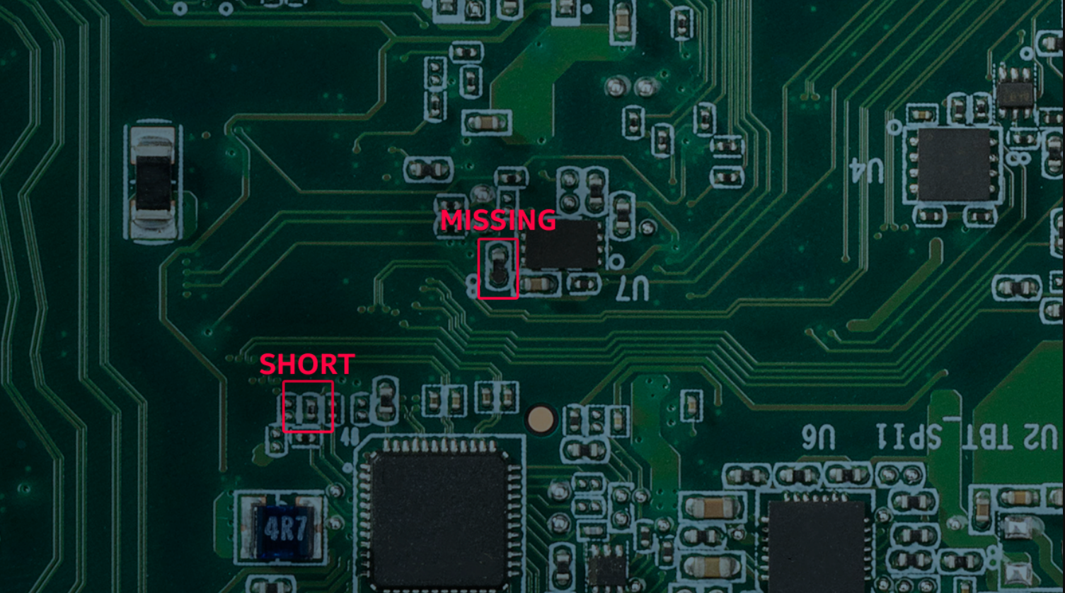
1. Incomplete coverage or pinholes
- Issue: Not only the inactive areas of the PCB may have a non-or inappropriate layer of solder masking cover, but they may also contain pin holes that expose the trace parts to the environment.
- Troubleshooting: Make the solder mask more viscous so it better covers the artwork substrate. Modify the printing factors, including squeegee pressure and printing speed, to guarantee the uniformity of the performance. Write your business thesis in about two sentences. Use more detailed stamps, formers, or masks to make it more precise. On examining the PCB computer board under the UV light, pinholes would be seen, and these areas could be touched with solder or ink masking as is manually applied.
2. Solder Mask Bridging
- Issue: Solder resist material between adjacent solder pads or traces, making a short circuit possible.
- Troubleshooting: Make the gaps between the hole pads and the slender lines larger. Develop the printing parameters that will allow you to maintain the solder resist material at the desired level. Check PCB conditions under the magnification lens after applying the solder mask, and use a proper fine tool to manually scrape off the solder bridges.
3. Solder Mask Delamination
- Issue: For instance, the solder mask can tear off from the PCB’s surface, leading to delamination (separation) or peeling due to improper adhesion.
- Troubleshooting: Make sure that the PCB surface is thoroughly cleaned and prepared for the solder mask by the process of cleaning. Attune the thermal profile, given factors like temperature and duration, to be able to ensure the proper binding of the solder mask material. Verify the compatibility of the solder mask material with the PCB substrate and any surface finishing controlled.
4. Color Variation or Discoloration
- Issue: Areas of the solder mask may appear color-changing or discolored, which affects the look of your PCB design.
- Troubleshooting: Keep processing parameters—temperature and humidity—unchanged during solder mask application and curing to achieve optimal results. Go for appropriate solder mask materials from reliable dealers in order to keep solder color variation at a low level. Perform routine quality control tests in order to watch out for color inconsistencies and spot any deviations as soon as possible.
5. Registration Errors
- Issue: Offsetting the solder mask with other layers of a printed circuit board, such as copper paths and component footprints, is another problem that needs to be taken into consideration.
- Troubleshooting: To have meaningful subtraction and alignment of the PCB, use high registration markers or registration pins during the fabrication process. Develop the envisioned program that optimizes the manufacturing process parameters for exactly the right solder mask layer placement and alignment. Install regular inspections and measurements to be able to confirm the correctness and identify any deviations.
What Are the Applications of Solder Masks in Optimizing Electronics Production?
Solder, solder mask manufacturers, and an important function in electronics manufacturing, work at almost all the production stages. Some key applications of solder masks in optimizing electronics production include:
- Preventing Short Circuits: The solder mask on a printed circuit board (PCB) offers an independent space between the adjacent conductive tracks on the board, therefore securing it from short circuits during assembly and operation. The probability of revision in the same work and part wear is thereby reduced, which leads to improvement in the production.
- Enhancing Solderability: A solder mask can ease the soldering process by detaching solder, which is not exclusively desired in regions like solder-masked regions. This allows the liquid to flow smoothly and results in the proper formation of joints during assembly, enabling manufacturing optimization and defect reduction at the same time.
- Protecting Against Environmental Factors: The main job of a solder mask is to act as a structural coating and shield a given material against moisture, dust, and chemical reactions. The solder mask coats the metal traces on the PCB that are left exposed, which shields them against corrosion by preventing the formation of oxidation and other forms of degradation over time that can compromise the reliability of the devices. This prevents unneeded prolonging of any component failure and makes the warranty claims less probable, bringing cost savings and better product quality.
- Facilitating Automated Assembly: The solder mask increases the automation of electronic assembly on the PCB when it provides visual differences and directions for placing it on the board surface. Furnishing pinpoint placement and soldering results in a decrease in requirements for correlation and the manufacture of products of uniform quality. Other than the purpose of the soldering mask to stop solder bridging, it also brings out some of the assembly issues. Solder masks are a contributing factor to efficiency in production activities.
- Improving Manufacturing Yield: Through the diminishment of defects like short circuits, solder bridges, or component misalignments, the solder mask ensures a rise in yield and production efficiency. It leads to a reduction in the number of discarded PCBs or the ones that are rebuilt, whereas the production costs and time it takes to bring products to market become lower.
- Enabling Miniaturization and High-Density Interconnects: The solder mask is indispensable for the micro-size and variety of electronic devices having their components interconnected in high density. It provides for delicate components with narrower pitches as well as detailed positioning, optimized board space utilization, and the chance to get elaborate electronic systems in one place. This is critical for making applications such as smartphones, wearables, and IoT devices where there is a need for very little space to be considered.
In particular, the solder mask plays a central role in the audio improvement process since it is a crucial manufacturing component that saves time, improves reliability, and allows other advancements in assembly. Its specific uses in PCB fabrication, final assembly, and various stages in between, through which electronic products in different industries will succeed, create an image of the product’s effectiveness.
Conclusion
This point could be summarized by stating that solder masks are one of the most vital elements of electronics manufacturing, which gives a lot of advantages, which in turn help to optimize manufacturing procedures and increase the reliability of electronic devices. Firstly, solder masks insulate the conductive traces, therefore preventing short circuits, and they are eventually protected against all the environmental factors that are assaulting the printed circuit boards (PCBs).
Also, its readiness for automation of assembly, improvement in solderability, and reduction in dimensional size cause increased manufacturing efficiency and higher production yields, as well as enabling products to reach the market faster. In summary, solder masks are an imperative element in present-day electronics production, having a balance of the crucial factors needed by the present technology: performance, reliability, and processability.


