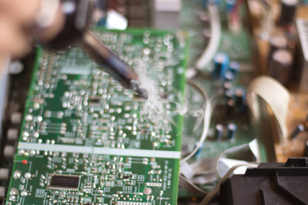
The soldering process is a step which is easy to master by beginner technicians and experts, and through it they can fasten kinds of components on the surface provided by the circuit boards. However, the solder in the high temperature environment can be non-wetting, which may cause low strength or unreliable solder joints. Comprehending why solder does not wet as well as identifying some its primary causes and implementing preventive action will help to ascertain successful soldering as part of your electronics projects. Dry soldering forms an essential process for many manufacturing industries, one of which, large scale production dominated by tiny components has copious risk of failing. Non-wetting issue, occurred rather frequently in the soldering reflow defects of PCB pads and pcb surface, might be a big threat to the boards’ strict integrity as well as permeate performance.
In this article, we’ll discuss avoiding solder defects such as the non-wetting phenomena and with the formation of strong and reliable soldered joints.
Understanding Solder Non-Wetting
Solder non-wetting is when molten solder does not distribute itself uniformly over the surfaces being welded. This occurs because iron oxide from the surface being welded is being pulled downwards by gravity and forms a barrier between the welding surfaces. The inconsistent joined activities can be led by many causes such as the dirty surface, wrong soldering temperature, not enough flux activity just like those degraded flux, and the incompatible materials.
What is a non wetting defect?
A non-wetting defect related to soldering happens when the molten compound does not wet completely or spread well over the metal surfaces that are being connected, which consequently leads to incomplete or weak soldering. When we say non wetting defects this is a type of soldering defect that will appear when if the molten solder solder will fails to bond with those base metallic bond in the board.
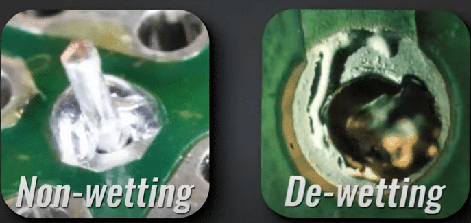
What is Dewetting?
When molten solder depicates from the service, this thus can leave behind well-patterned solder marks. As this may be caused by contamination, overheating or incorrect flushing, it can result in reduced joint life, and as a consequence, prolonged energy use and even structural failure.
Non wetting vs Dewetting
Non-wetting and dewetting are phenomena that appear during soldering, though they are not in the same order and have the reason and consequence. The both of them can be prevented with good soldering practices to use plus the optimization of material preparation.
Non-Wetting:
- Definition: The condition known as non-wetting occurs when solder melts and does not evenly wet the full surface of the materials needing soldering thereby resulting in improper or weak solder joints.
- Causes: It may have roots in surface contamination, incorrect temperature of soldering, inactivized flux, or the unmatched materials being used.
- Effects: This results in insufficient welding, and the joints may not be able to perform the function nor sustain the reliability of the entire electronic assembly.
- Prevention: Proper surface pre-treatment, the flux selection, temperature control of soldering and the use of appropriate alloys which do not form non-wetting can be fully effective.
Dewetting
- Definition: Dewetting occurs if molting solder is not properly distributed around the surface of the solder pad, leaving some spots with no or little solder.
- Causes: These may include, but are not limited to, overheating, masonry work overhaul, or the influence of external pollution.
- Effects: The bonding process deteriorates as a result of losing the melting tendency of the tin which causes the joints between the electronic components to weaken which subsequently can lead to electrical and mechanical failures in the circuit.
- Prevention: The dewetting might be changed by regulating the soldering parameters, having the right flux, better surface preparation and pollution prevention.
Why it’s important to fix non wetting defects
Repairing soldering fractures is vital as they may result in incomplete or weak joints being formed, which will in turn lead to the inefficiency in the performance of electronic assembly products. The consequences of a solder joint that is improperly implemented can be electrical resistance, intermittent or component failure which in return leads to the expensive repairs or production failures.
What are the common causes of non wetting defect?
Common causes of non-wetting defects in soldering include:
Surface Contamination
The existence of oxides, crude oil, dirt and dust or other impurities on soldering surfaces have the tendency of stopping solder’s wetting.
Improper Flux Activity
The case of inefficient or insufficient flux could be incapable to remove the surface hoods and create a good wetting have a good solder joint fillet.
Incorrect Soldering Temperatures
The soldering process to be slow by not attaining temps required to melt and flow the solder or either preheat temperature will most likely cause wicking, non wicking like inconsistent soldering temperatures.
Incompatible Materials
When there is a non correspondence between solder alloy and substrate materials there is a possibility of inefficient solder and substrate wettability.
Surface Finish Issues
Some finishes, such as OSP (organic solderability preservers), when subjected to base metal surface belonging to the solder alloys may degrade or not be in accordance with the nature of these types of metals. Consequentially, the solder alloy does not properly adhere to the surfaces, such as non-wetting.
Poor Solderability
Surfaces characterized with low surface tension might have a tendency to shed solder hence no proper wetting can be achieved.
How to correct non wetting defects?
To correct non-wetting defects in soldering occurs others to prevent non wetting defect, you can take the following steps:
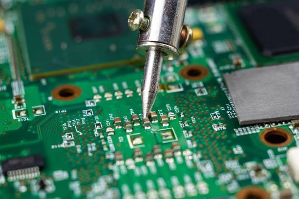
Surface Preparation
Carry out the activity of soldering but make a point that the surfaces to be soldered are clean and free from any contaminants. Use the efficient cleaning procedure for the best results, use ethanol or a flux cleaner.
Flux Selection
Choose a grade flux with good performance and have the same strand as solder alloy and substrate kinds. The solder flux must be a good wettability agent to ensure solder joint is being properly encapsulated.
Soldering Temperature
For the solder alloy being soldered on, confirm that the soldering temperature is in accordance with the recommended range. Prevent the formation of non-wetting screens by making sure that the temperature is neither very low nor too high.
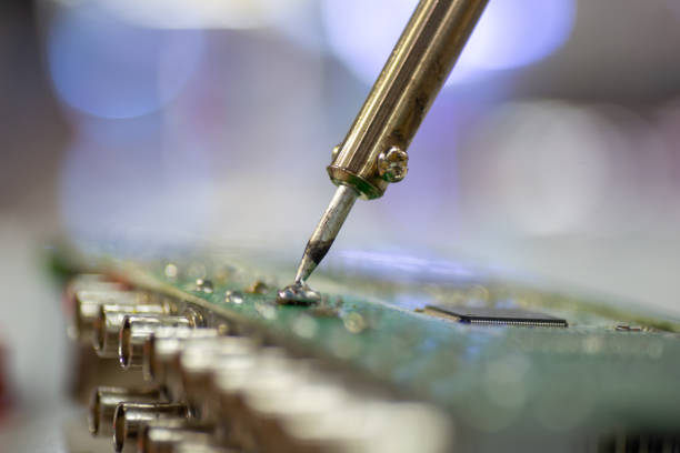
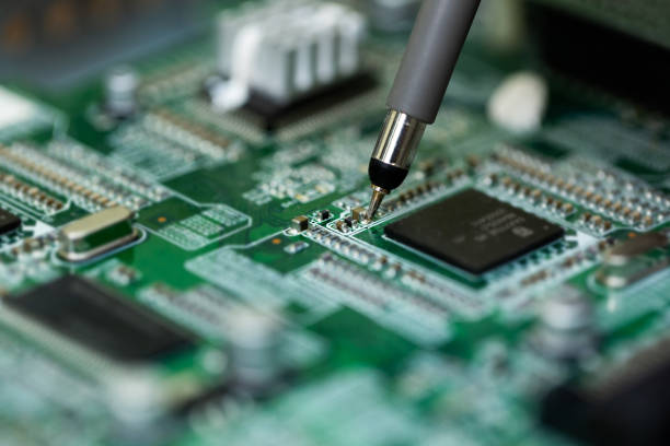
Soldering Technique
Always practice the appropriate soldering technique like applying the soldering tip to the joint but for having it kept on for just the right time. Stray away from using similar term excessively pressure which could result into non-wetting, the surface repelling water.
Component Placement
Be sure to put each part in its right place and to align them rightly before soldering. Different components because of the misaligned structure can make connecting gaps that hinder the proper solder wetting.
Avoid Excessive Solder
Make sure you have used the right amount of solder for the joint. Too much solder will affect the solubility as the wavy trace will give space to enable solder to pool and vice-versa.
Avoid Contaminants
Ensure the soldering area is a clean place for the application of solder is not affected by the outside contaminants. Make sure to use containers that don’t let air in to prevent contamination of solder and fluxes.
Quality Control
Accept quality control measures to check the solder joints are properly sufficient wetting and to identify other defects. Use magnification and testing equipment to check how strong bondings are between solder joints.
What causes poor wetting, and why is it a problem?
Causes of poor wetting in soldering include contaminated surface, inadequate activity of flux, insufficient working temperature, as well as incompatible components. It is a problem as it can weak or incomplete solder joints. They eventually become inoperable. These typically give better wetting, especially for soldering difficult surface finishes or oxidized surfaces. There is a mismatch between the plating layer material and the applied solder paste.
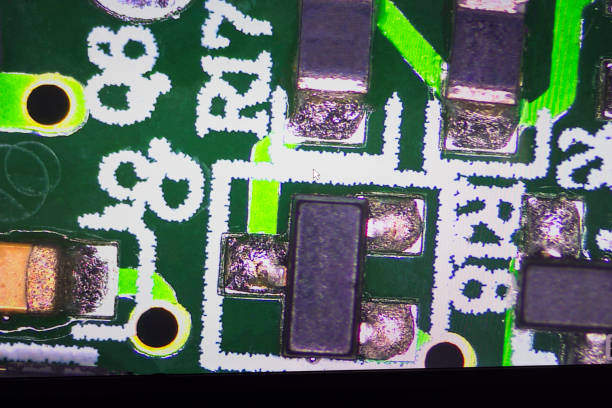
Causes of Solder Non-Wetting
Insufficient Solder Paste A low volume of solder paste frequently causes non-wetting because an adequate spread of solder paste is necessary for ensuring stable solder joints.
- Contamination: Contamination is one of the important causes of solder bad wettability on the surfaces being soldered. Protective oxidation films, flux residues, oils, or other contaminants possibly stay at the surface during soldering, therefore this could prevent the solder from maximum wetting properly and leave cracks and or voids.
- Surface Finish: The quality of the surface finish of the substrate can also influence the appearance of the solder. Some surface finishes, e.g. OSP (Organic Solderability Preservatives), can be harmful for the environment and their effectiveness varies. They might not even be compatible with the soldering alloys, making the solder balling less effective.
- Temperature: Soldering is not resistance to significant temperature. If the temperature of soldering is below the melting mark, the solder may not get liquefied enough which means it will not flow. This results in the non-wetting of the component. Alternatively, high temperature conditions might make the substrate and components to degrade thermally and hence non-wetting tendency to surface might also occur either if have insufficient soldering temperatures.
- Flux Activity: Flux does this by cleaning the surface and by acting as a transport agent hence solder can flow towards the interface between the copper surface and the applied solder paste. This issue may be due to poor flux or poor solder wetting application or its ineffectiveness that causes non-wetting issues.
- Surface Energy: The nature of bendability by solder joints depends on surface energy of substrate material. Materials with low surface energy may remit the solder from the surface, therefore not letting the solder exert precisely enough pressure to form a joint.
Solutions to Solder Non-Wetting
- Surface Preparation: Good cleaning and removing of contaminants from the surface to be soldered with a variety of methods are very important to avoid the contaminants’ hindering the solder wetting or solder wetting behavior. It can be carried out, for instance, by using cleaning agents, mechanical or plasma-based approach.
- Optimized Soldering Parameters: For the soldering operation to produce quality results it is important to know the right soldering temperature, time, and pressure to use based on the materials to be soldered.
- Flux Selection: properly identifying the required flux is a crucial action. The flux and the solder alloy should be compatible, and there should be a right amount of activity to eliminate the surface oxides and it helps the wetting.
- Surface Finish Selection: When choosing a suitable surface finish that works well with the caving solver and still has excellent wetting properties, it can be a useful way to avoid solder non-wetting.
Solder Alloy Selection: Suppling the alloys of solder which are well-known to demonstrate good wetting properties is another way how to avoid the problem of soldering non-wetting.
Wetting of solder pastes can cause some difficulties in electronics manufacturing but by getting acquainted with the reason behind this and the possible ways to confront the issue, it can be solve. The correct surface preparation, choosing the appropriate temperature parameters, flux and soldering alloy, surface finish and the right solder alloy are leading factors in creating solder joints with the required reliability and integrity level and also don’t use expired solder paste..
Dispelling the Black Magic of Solder Paste
The stranger could be the solder paste that as engineers we consider to be amazing, it plays an important rule in electronics production. Yet, comprehending its substances and meaning can debunk the disablement of its behavior and the better ends to printed solder paste the performance.
Solder paste, a combination of soldering powder and flux, is stirred here. In our case, the solder powder will be mainly prepared using the standard combinations: tin, lead and other alloy-based components such as alloy solder joints, while the flux is a chemical agent that cleans and prepares the surfaces some have contaminated flux. As a result, the process that occurs at the beginning of heating, the flux activates that removes the oxides and dirt from the surfaces, and finally, during this process, the solder will be able to flow and bond. Solder requires a certain thermal threshold to bond properly with the base metal.
The flux is required to lead free solder alloy to an excellent spread when the solder is applied on the surfaces to be welded. It reduces the surface tension of the molten solder or molten solder coats, letting it fill all cavities equally on the surfaces of the various components. Flux can be used to clean up the surfaces, thus, the accumulated oxides might diminish the process of solder wetting and the flux in the solder paste evaporates more quickly thus affecting the wetting properties of solder paste when using the same reflow profile as well as an oxidation layer (oxide layer or thin layer) prevents contact between the solder and the surface plating layer.
Solder paste is a vital input in electronics manufacturing chain that allows forming the strong and responsible soldering joints. The plating thickness is too thin or the result of poor processing, which can be easily damaged during assembly; The soldering temperature is not high enough. The comprehension of the solder’s bonding mechanism, functionality, and use enhances your ability to differentiate between solder paste and sorcery, therefore, welcoming it as an important and versatile asset in the modern electronics packaging industry.


