Screening, or silk screening, is an inseparable part of printed circuit board (PCB) decoration due to its graphics and text capabilities. It is a versatile and low-cost technique, which makes it possible for us to develop complex PCBs that are durable enough to withstand the most rigorous usage conditions.
In our comprehensive tutorial on silk screening on PCBs, we will take you through the steps involved in it and screen printing, as well as the basic and advanced techniques that can help you achieve professional results.
What is the Silk Screening PCB?
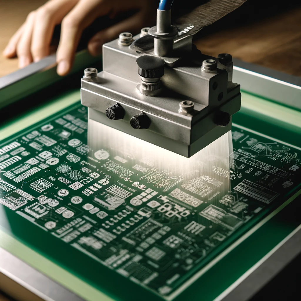
Stencil printing of PCB is exactly that: paint film is laid over the PCB through a particular stencil. The stencil will then be laid over the PCB, and ink will be applied to this by forcing the ink through the stencil onto this board using a squeegee. The act of ink deposition in this process will embark on an exact definition of the lines, text, and graphics, hence being fit for use in PCBs.
The importance of the silkscreen PCB to the assembly process:
Component Placement
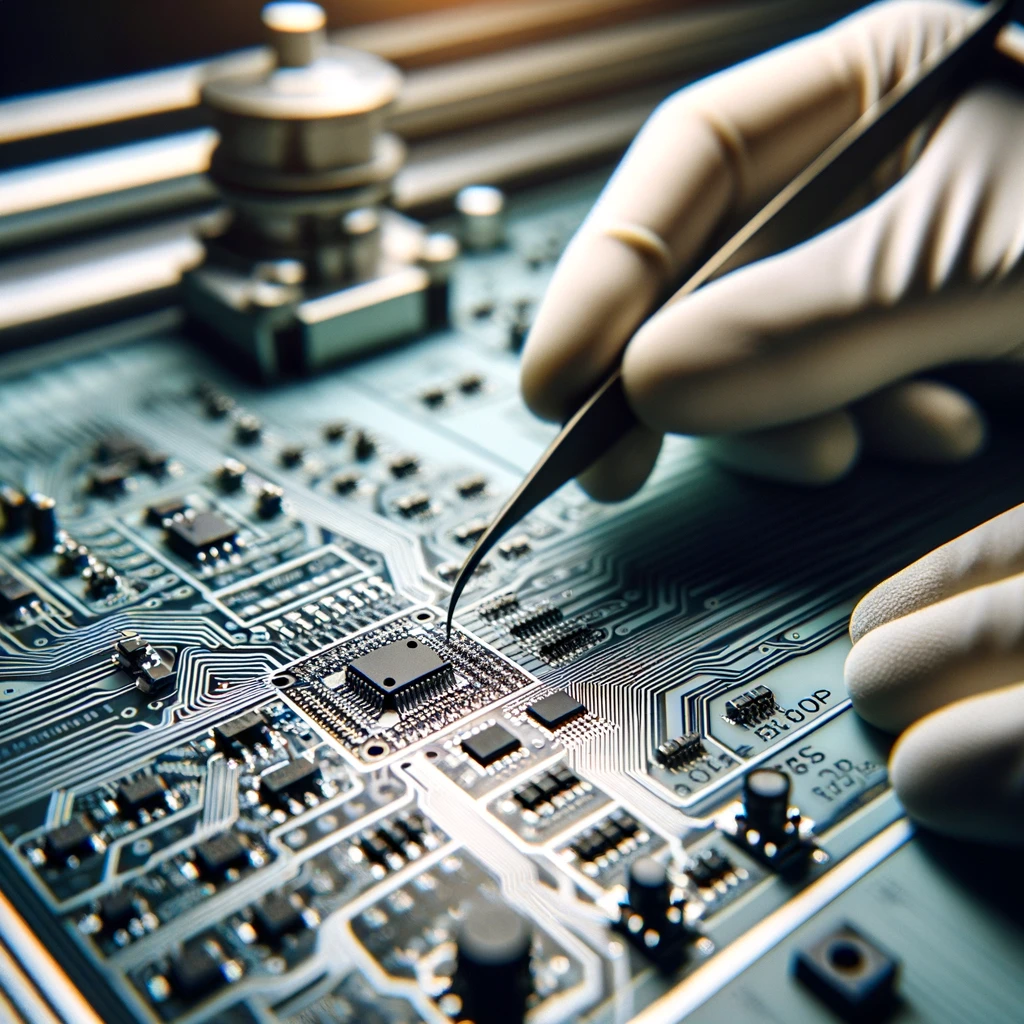
Silkscreening of the PCBs is a crucial element in determining the correct array of devices on the PCB. Reference designators that consist of symbols alluding to the pcb components type and position (R1, C2, etc.) minimize the error of misplacement during assembly.
Orientation and Polarity
Let me zoom in on this silk-screen print of a PCB so you can see where to place the components. Make sure the arrows show the way the electron flow goes in the circuit, and the lines mean where you should put the component body. The accurate definition of these parts is provided in the photo. Moreover, the plus (+) and minus (-) signs are marked to show the orientation of the components, such as capacitors and diodes, towards these symbols during correct assembly or installation.
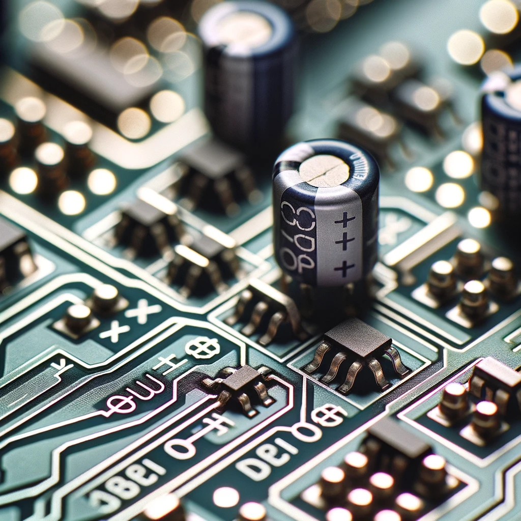
Silkscreen markings The symbols on silk screen serve as the orientation and polarity manifestations of a component, for instance, diodes, capacitors, and ICs. Appropriate sequencing guarantees that components can be placed accordingly; hence, it minimizes the risk of assembly mistakes.
Troubleshooting
It is a visualization looking at an engineer as he grapples with the concerns about the silk screening method on a printed circuit board (PCB). This picture shows technicians utilizing magnifying glasses and other tools to check the PCB for any offset, smudging, or uneven ink distribution in a silk print layer.
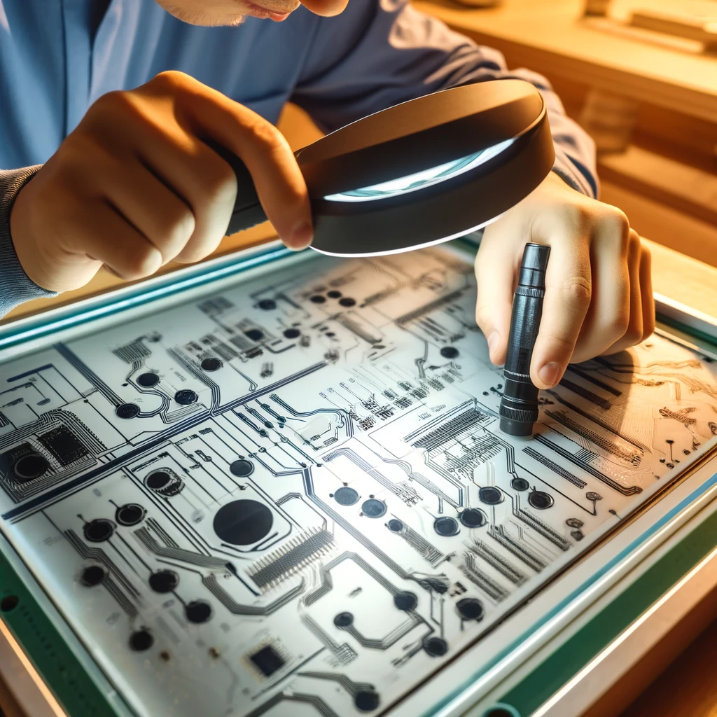
Test points and other diagnostic information can provide tips for assembly problems and may cause troubleshooting and debugging of the of the assembly process. This may involve traceability of parts, identification, and resolution of problems before they turn into serious downtime and production disruptions.
Quality Control
Take a look at the photo of the silk-screened printed circuit board (PCB) with its incorporation of reliability facts like production date, manufacturer’s serial number, and revision interpretation. The photograph, through the lens, evidently shows all of these aspects, highlighting the utter ivory of the silk-screened words and figures.
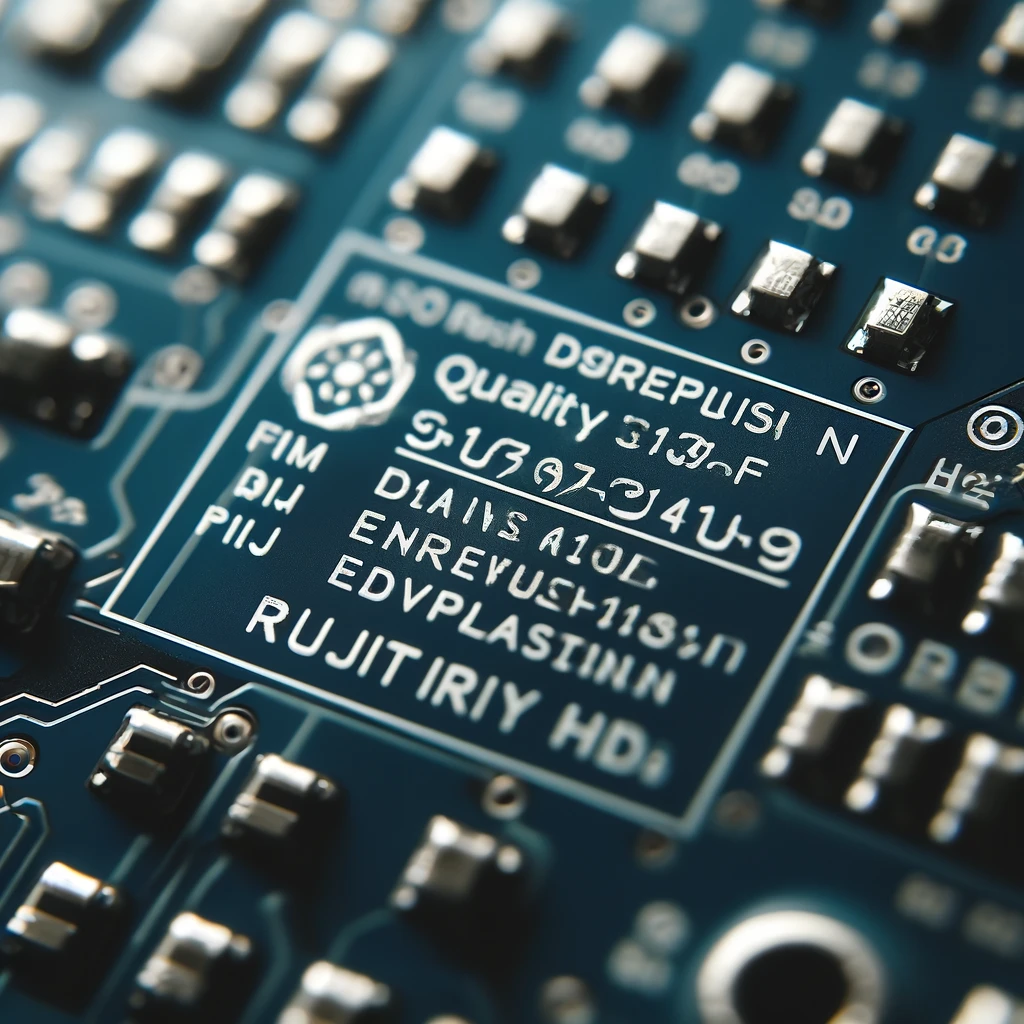
It is also possible for silkscreen PCBs to contain quality elements such as the production date, manufacturing serial number, revision explanation, and so on. The guide further safeguards against misassembles and ensures that the many electronic components are of the correct specifications. Furthermore, it streamlines problem identification where there may be a need for equipment replacement.
User Instructions
This is an enlarged picture of equipment for silk-screen printing a printed circuit board (PCB), which includes the customers’ guidelines and safety data. The screenshot makes it very clear that the text and icons of factory settings and safety precautions are displayed. These characters should be made as legible as possible, as should the location.
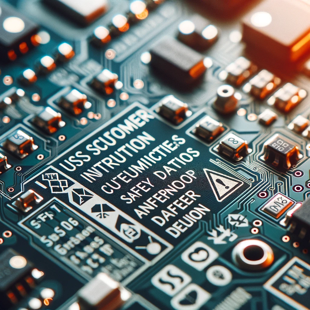
Occasionally, silkscreen PCBs may contain customer’s instructions or even safety data when it involves consumer electronics. This is printed text and is hence strategically placed on the PCB to double as a user manual for the end user and can be referred to at any point during the operation of the device.
What are the functions and significance of silkscreen?
Silkscreen, the other name for legend printing, on printed circuit boards (PCBs) is beneficial in some major aspects of the manufacturing and assembly of such circuit boards. The block diagram is a key source of information for human assemblers, enabling the smooth connection of circuits and easing the repair and maintenance procedures for electronic devices. Here are the key functions and significance of silkscreen on PCBs:
- Component Identification: The silkscreen instantly colors the outer-layer parts of the board.
- Orientation and Polarity: Its silkscreen is particularly useful for product orientation as well as component polarity.
- Assembly Instructions: Stencils may also contain connection rules and soldering information.
- Test Points and Debugging Information: The silkscreen consists of test points and a debugging illustration for running the diagnostics.
- Quality Control and Traceability: The silkscreen carries the quality control specifications, date, and traceability information as a part of the product information.
- User Information: The silkscreen will provide the product name, model number, safety instructions, and warning label.
PCB silkscreen printing process
In silkscreen printing of PCBs, one can get a lot of steps and accurately see their markings and text as a printed circuit board (PCB). Here’s an overview of the PCB silkscreen printing process:
- Design Preparation: Before the next stage begins, the silkscreen art must be prepared by the designer with PCB design software. This layout has component outlines, designators, test points, and other information about the important components.
- Stencil Creation: Each silkscreen layers is made using a stencil for the silkscreen layer. Generally, the stencil is either polyester film-based or metal-based and is intended for applying ink to the PCB.
- Ink Preparation: This mixture is then made thick enough to get the required hue and consistency. High-value silscreen-printed inks are created for PCBs to ensure flexibility and sticking power.
- Cleaning the PCB: In order to be printed by silkscreen, the PCB is cleaned first to remove any dust or dirt nuisance.
- Screen Printing: The stencil over the PCB is perched, and then ink is made to flow using a squeegee to the screen printing process. The ink is being forced through the mesh all the way onto the PCB, etching the silkscreen print pattern in the process.
- Curing the Ink: Then, after the ink is prepared, the board is taken into the oven, where it is cured. The ink cure, for this, is a must; hence, it ensures the ink sticks tightly to the PCB and is resistant to wear and tear.
- Inspection: If there is any error, after the ink is dry, the screen will be checked and reprinted if it does not meet the required standard. All the faults and mistakes are debugged before going ahead.
- Final Touches: The whole PCB is then inspected, and the excess ink and dirt are removed from it. With the silk-screened PCB assembly jobs completed, the parts can now be mounted on the board.
The silkscreen PCB printing process is quite demanding and requires precision and full attention to details to get the marks and text well treated and positioned properly. By taking into consideration these points, the same manufacturer will be able to come up with a good silk-screening design, which helps in the efficient assembly and checking of the PCBs.
Methods of Silk Screen Printing
Silk screen printing machine (or screen printing method or serigraphy for a longer name) is a popular old-style printing technique for picture transfer to different objects. Here are the silkscreen method involved in actual silkscreen printing:
- Preparation of Screen: Within the scope of the procedure, a screen has to be prepared, which is made of either silk or a synthetic mesh stretched tightly on the frame. Then the screen gets coated with a red-sensitive emulsion.
- Creating the stencil: A stencil, which is created on screen by masking the areas that should not receive the ink, is called a screen. This can be done in different ways, using many techniques like printing hand-cut stencils, photo emulsion, or digitally.
- Preparing the Ink: Ink or paint is produced by combining different pigments with a binder so that it becomes suitable for printing the printed piece. There are a variety inks; ideally, each material / application has its own peculiar ink.
- Mounting the Screen: Then the prepared screen is fixed onto a printing press, which in turn presses down on the material to be printed.
- Printing Process: However, ink will be neatly placed over the screen with the use of a squeegee, which is the tool that makes it spread evenly. When the squeegee is moved across the screen, the rolled-up ink is forced into the open space of the stencil and onto the material underneath.
- Curing the Ink: After the ink is placed in a base, it has to be cured so that it does not smudge. Washing and drying the ink can also be accomplished by applying heat, UV light, or air drying, depending on the ink type.
- Repeating the Process: The colors for multi-color silkscreen artwork design are made separately for each color in the screen printing. This procedure is subsequently carried out for the succeeding color, with careful alignment to keep the final work right on track.
- Finishing: The screen may be perfected further until the actual printing, by designing a heat set (drying) or washing and processed through these stages to avoid cracks.
The silk printing technique is a versatile method for which you are most welcome to spend your budget in a healthy way. It is allowable for multiple materials such as paper, fabric, glass, metal, and plastic. It is represented with a very high colour quality and its long life is highly determining for many printmaking processess.
Factors to Keep in Mind When Designing Silk Screen for your PCB
While considering the silkscreen on your printed circuit board (PCB), there are several issues that need to be taken into account for the entire process do accomplish its expected results. Here are key considerations:
- Clarity and legibility: The silk-screen process has to be clearly written and it should be in good visibility, with proper contrast it has with the substrate materials. Clear component designators and thereby other information should be located on the PCB substrate.
- Component Placement: Stipulate that the silkscreen does not cross out the part(s) that were placed. The process of creating mechanisms which are of the appropriate size for the areas where they will operate should be done in better conditions.
- Orientation and Polarity: Inspect the circuit board quite visibly for all components and their placement direction so that assembly mistakes are not committed.
- Line Width and Spacing: The text and graphic placement which are parallel and no gaps in line width and spacing is also appropriate. They are neatly placed.
- Color Selection: Determine what color will be noticeable enough and consistently presented on the PCB outline. The bright white printed circuit board will make it easy to check for soldering errors or errors on the solder mask at this stage as it provides the best contrast to the rest of the PCB.
- Test Points and Reference Designators: Apply test points, as well as reference designators for technicians to trigger devices for trouble shooting and identify components.
- Quality Control Information: Insert a system which includes the manufacturing process date, batch or number, and revision numbers that allow to trace and ensure products’ quality.
- Compliance and Regulatory Information: Access is provided to all signs, instructionals, and marking labels, including the CE and RoH symbols if they are necessary and applicable.
- User Instructions: If it is necessary, include the user guide or some safety tips about the product in a silkscreen image with a detailed explanation to help the buyer have a good grasp of its safety precautions.
- Aesthetics and Branding: Consider the branding of the entire “silkscreen,” for example the printing of a company’s logo, a caption and/or maybe your brand name.
Through all these designing elements which are mentioned here, it is ensured that at first and foremost a professional and consistent product will be delivered, and on the secondary side, it also stipulates a good documentation, testing, and maintenance operations in the industry.
Types of PCB Silkscreen
Regarding the many types of PCB silkscreen methods used in the global electronics industry, they can be distinguished by the procedure they use especially in liquid photo imaging lpi, inkjet projector and direct legend printing dlp. There is an array of methods, and each is put to use for a particular requirement in designing a printed circuit board. Here are some common types of PCB silkscreen methods and to the pcb silkscreen manufacturer:
Hand-Screen Printing
Inside is a visual of printing by hand using silkscreen onto a printed circuit board, or PCB. The picture shows a technician physically laying down the screen print ink using a squeegee, but at the same time, trusting the stencil on the screen and rectifying the ink deposition of the PCB into the board.
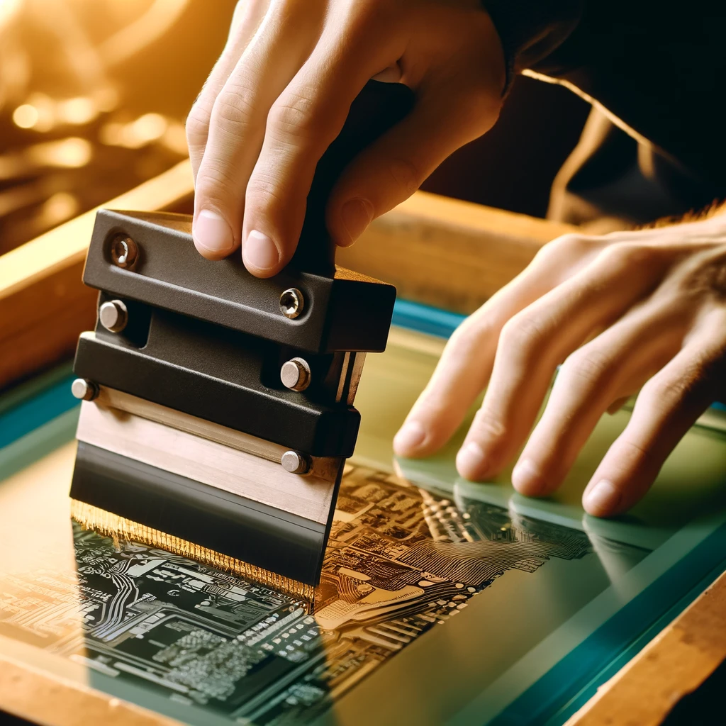
This is a manual method where the ink is applied by a mechanically driven squeegee over a stencil placed over the PCB fabrication. Manual screen printing is good for a short production run and gives the possibility of modifications throughout the design.
Automatic Screen Printing
The following picture, almost touching, is the making of an automatic screen print on a printed circuit board (PCB) by silk screen process. The photo tries to give the viewers a glimpse of the automatic machine when it acts; mainly, it deals with the mechanical elements like the squeegee trailing over the stencil to impart ink onto the PCB.
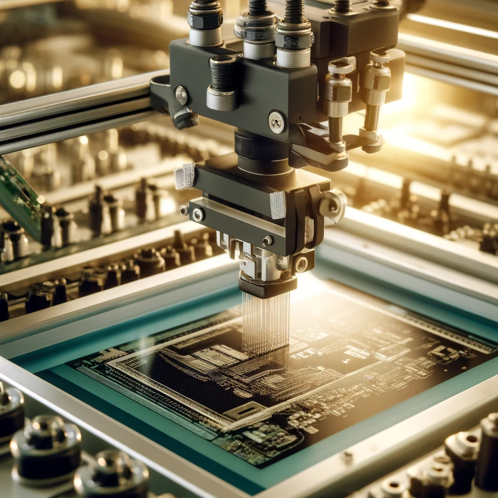
In this printing technique, the image, design, or letters are transferred into a machine where the silkscreen process takes place. Speed and accuracy are its main benefits, which make it a better fit for large-volume printing than hand-printing.
Digital Printing method
This image highlights the digital printing process for printed circuit boards (PCBs). Here, we see how the blank boards are automatically loaded, ready to be passed through the digital printer. The photo has such a tense spot the moment ink is put on the PCB under the print head with the planned pattern of circuits.
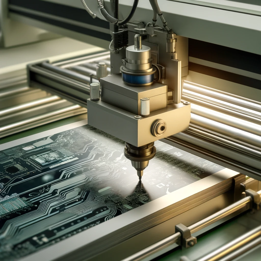
Digital printing, as it is called, is carried out by the PCB sheets being passed through the printer. The high resolution and unique applicability for complex design and prototyping visualization make the tool a real advantage.
Stencil Printing method
This figure shows the stencil printing process that happens on a printed circuit board (PCB) producing silkscreen image. The shown picture revealed that solder paste is being brought into the PCB through a stencil by the squeegee. The paste is fomed in the pads by the filling of the tiny holes of the stencil and the pad is used for the component mounting. The art of weaving through the picturing of the precision and the detail of the process clearly exposed there.

The stencil printing technique consists of stencils and ink to form the final product. It increases accuracy, which is why it is appropriate for general tasks and small components.
Inkjet Printing method
Inkjet printing, which is non-contact and directly places the ink onto the PCB, is a popular process. Such a print technology is suitable for the highest quality printing, and it does have possibilities for complex patterns such as acrylic ink.
Laser Printing method
The following is an ultra close-up picture of a laser printing method during silkscreen labelling with a printed circuit board (PCB). The picture is shot from the aspect of the laser printer working, and we can focus on the laser beam which applies the permanent and accurate notes for manufacturing and wiring purpose on the PCB.
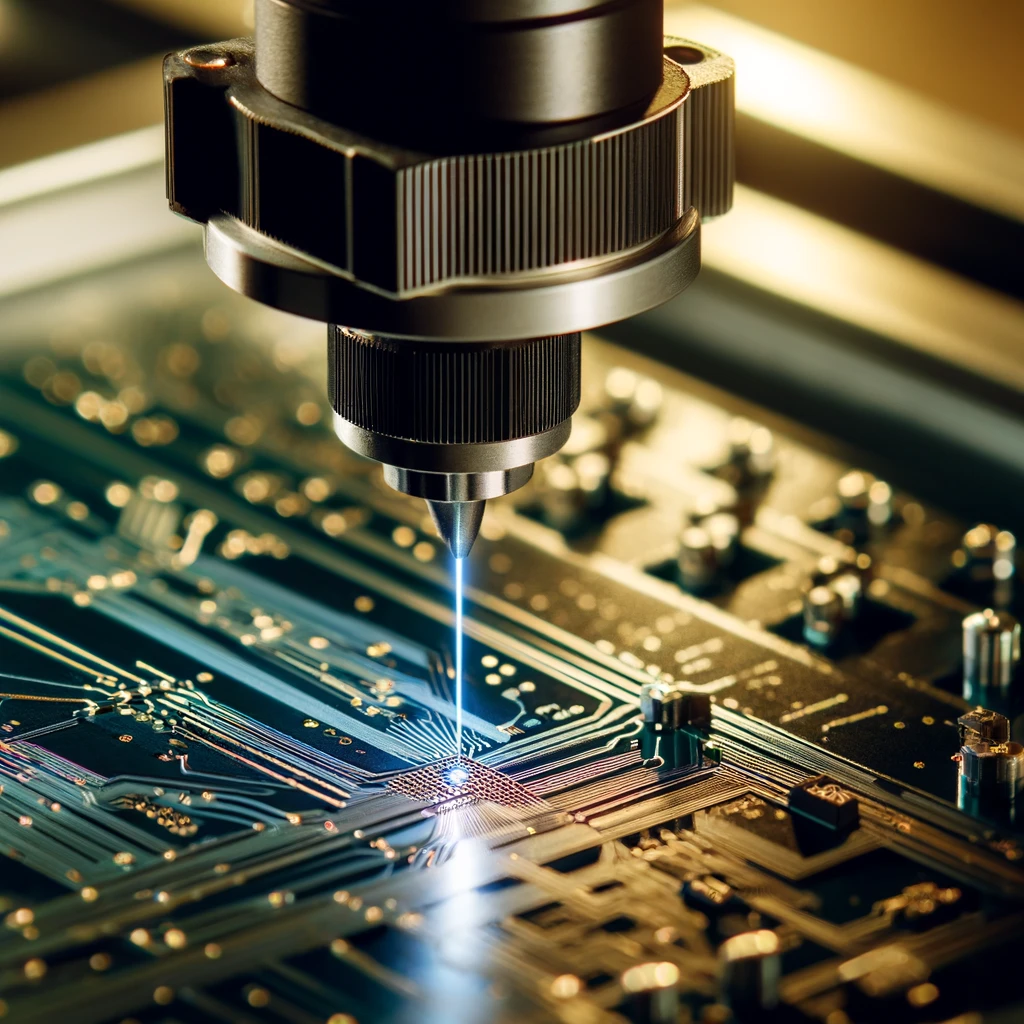
Laser printing, via intense laser rays, applies toner to the PCB. Having a good resolution and found when do prototyping and small production runs, it is appropriate for high-resolution printing.
Different ways of silkscreen for PCB comprise the respective advantages that are threfore dependable on the factors such as the quantity of the productions, the complexity of the designing needed and also the budget some have direct legend printing. Knowing and grasping the different PCB silkscreen helps methods will ease the work of a designer for a particular case.
Manual Screen Printing
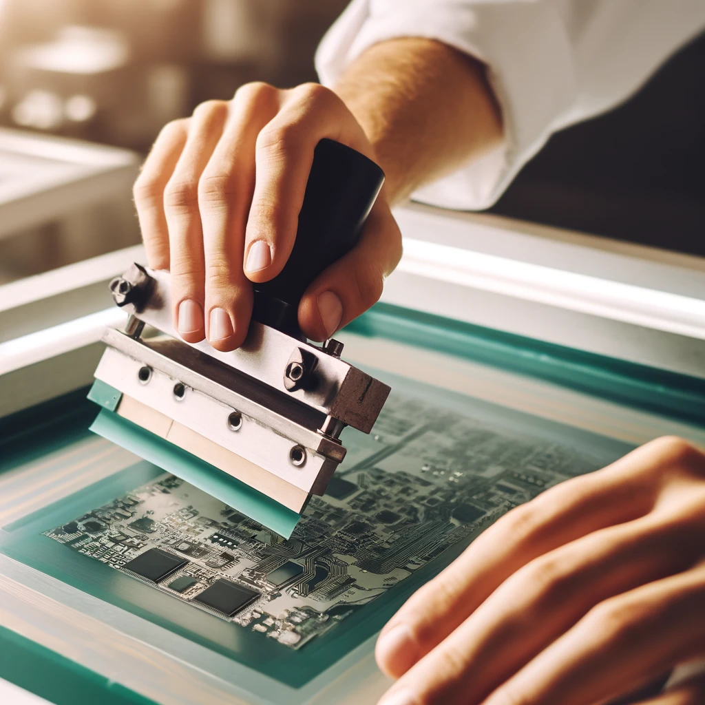
Manual screen printing is one of the classic techniques that cells use to extrude (or inject) the screen onto the mesh with the help of a stencil. It consists of the masking process, filling ink, and transferring the ink traces from the printing plate to the base through squeezing prints. Manual/hand-screen printing produces a multitude of cost-effective silkscreen designs and can be used on a wide variety of materials. However, it can be tiresome work and may take longer to print highly detailed designs.
What are the benefits of using silkscreen on a PCB board?
- Cost-effective: Silkscreening is a budget-friendly and even more suitable practice that applies to PCB manufacturer with text and graphics not only in major productions but also in small productions.
- High-quality results: The hand-crafted silk screen printing will compete with other long-lasting, good-quality prints.
- Versatile: Silk screening also offers a diverse toolkit for design; even plain text can be incorporated with complex graphics.
- Customization: The element of silk screening makes PCB surface customizable to a large extent, thus perfecting prototyping and a small production run.
Advanced Techniques for Silk Screening PCB
- Multiple Colors: The silk screening printing can print the designs that come in multiple colors by using various stencils and printing each color using a separate one.
- Fine Details: In this case, the finer mesh fabric and thinner ink will be the best choice for more fine-detailed prints to be crisp.
- Special Effects: Gilding can be achieved by the print screen technique as a special effect with the help of paint of silver and paint of corrugated.
Conclusion
Silk screening, as the name indicates, is also turning out to be a versatile and cost-effective option for adding graphics and text to PCBs. Through your excellence in silk screening operations, you can make quality and custom desktop circuit boards suitable for many fields and applications or in non-conductive epoxy ink. Either you’re an enthusiast with a desire to create a PCB silkscreen process to match your projects and save costs or you’re a professional PCB designer seeking a reliable means of producing high-quality boards, the silk screening technique should definitely occupy your attention, as should DIY PCB silkscreen.
