Printed Circuit Board (PCB) plays role of a tireless and invisible “working hand” that turn the electrical “pieces together”. Distinguishing among many complicated PCB fabrication processes, via filling occupies a very important position by what it affects the end result to be reliable and have good performance. In the next article, let’s study what is a PCB filling, know which one is more important and which one is not and best practice for each.
The main insight of the study will be the significance of PCB’s through designing advanced, durable and effective circuit boards. Experience how the unknown becomes clear through the explaining of core elements in PCB making.
Understanding the Role of pcb Via filling
Vias as are the small holes that are drilled thru PCBs to achieve electric connection between various other “ inner layers”. Such ones are crucial for the board ability to perform their primary duty namely allowing signals as well as electricity to flow among components. Along with the aforementioned portion, a filler is also required in cases where there is excess mounting holes. A conductive material is used which not only facilitates reliable electrical connections but also enhances the mechanical strength of the board.
What is via hole filling or plugging of a pcb assembly?
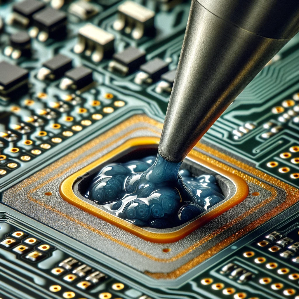
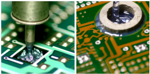
Hole-filling or Plugging in the through-hole process is the way of packaging the holes (via) with a material and then protecting it against environmental factors such as corrosion and other factors thus its electrical and mechanical properties will be improved. It means that this is a process where the via hole walls is filled or round the solder mask or resin. And then, when the via hole wall are being filled or plugged to gain improvements the pcb assembly which is reliable by lowering the possible trapped of air or liquid in the via filling, and then by ensuring a good yield thru pcb assembly.
What is Via filling process?
Throughput is a via filling process in printed circuit board manufacturing, which instructs the filling of a via hole on the boards with either conductive or non-conductive components that enhance structure and electrical connectivity. Often filleting involves making sure that the power PCB board is cleaned before applying the filler that later is cured or solidified to reinforce the connection between various parts of the PCB.
What are the types of via filling?
As there exist a variety of methods used for via filling in a printed circuit boards, they can be broadly divided into some categories each with its own strengths and weaknesses. Some of the most common methods include:Some of the most common methods include:
Solder Mask Filling material
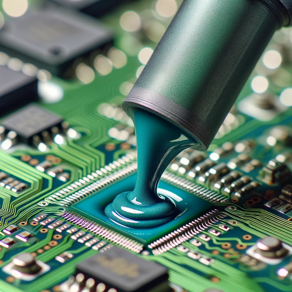
This is done by coating the via solder with solder paste, and subsequently, will be placed in the reflow oven to be bonded together. Following reflow soldering, which is conducted on preheated boards, the excess solder is removed. The final product is a via, which is filled. This method is inexpensive and has wide applications by two-layers in circuit layers of buildup by small to medium-sized vias.
Conductive Paste Filling
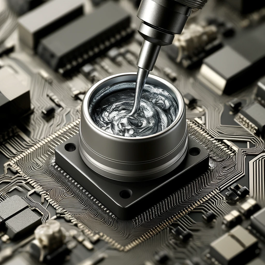
Fill the vias by using catalytic pastes (silver epoxy or copper composite epoxies or copper conductive epoxy or copper or silver epoxy). The pastes are then would be employed to fill the buried vias, and cure process to allow the paste to form a solid conductive path. Using these techniques, power can be efficiently conducted. Therefore, this process may cost more than other methods used instead for similar purposes.
Electroplating
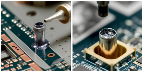
One key method is the electroplating procedure. This involves the application of very thin layer of metal like copper pad in the via, using an electrolytic process either an active pad. This method enables high level filling and thus rendering it suitable for high-density flexi boards and high-frequency circuits.
Resin Filling
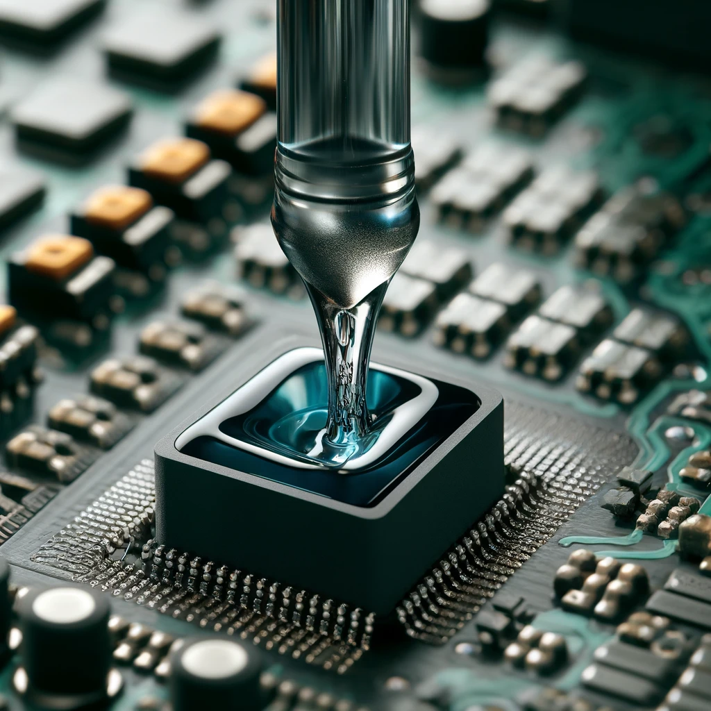
The resin filling solution refers to a similar process where epoxy resin is the dielectric material that is used to fill the via. The approach can deliver a good mechanical support with an aim of providing stability to the board but it is not applicable for the high frequency case due to its dielectric nature.
What are some key benefits of filled vias?
Filled vias offer several key benefits in PCB manufacturing:
- Improved Reliability: Putting drills reinforces the strong bones of the printed circuit board, minimizing the probability of breakage from stress dealt by mechanical forces or impact of environmental elements.
- Enhanced Electrical Performance: Filled viashold the electrical connection generating a more reliable electrical conduction while signals are not lost and signal integrity is improved.
- Thermal Management: Vias full up also finds use in thermal dissipation thereby working towards advancing the thermal performance of the printed circuit board.
- Improved Solderability: Added to this, the filled vias can improve board solderability providing easier assembly of the boards and consequently this can significantly reduce solder defects risk.
- Mechanical Support: This type of vias contribute toward providing additional mechanical support or wiring structure for components mounted on the board, thus reducing the impact of vibration or shock produced thereby.
What is Conductive filled vias?
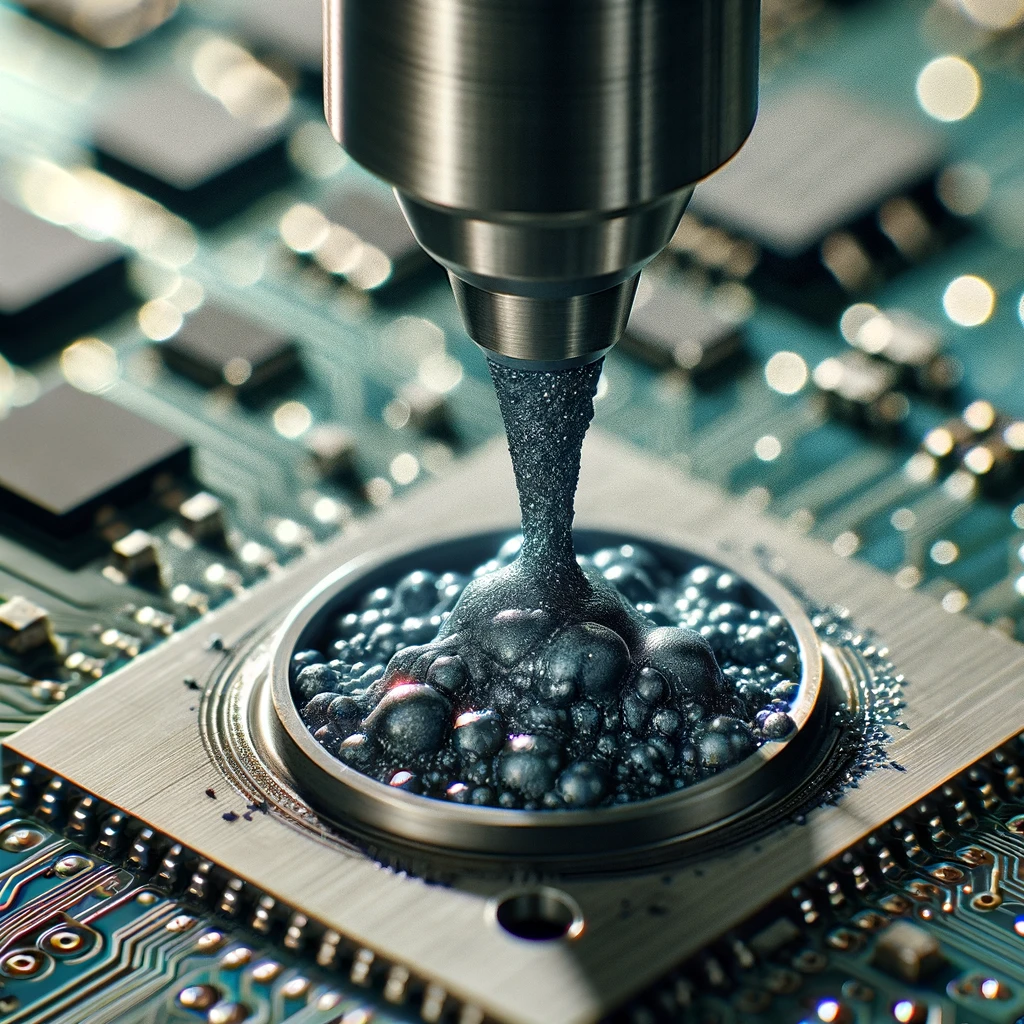
Through-vias which are filled are vias in a PCB being filled with conductive materials like copper or conductive epoxy. Thus, these vias act as low-resistance conduits, and hence, allow the he signals to flow between the layers of the printed circuit board that boosts the physical board’s performance on the electric front. Conductive filling vias are known for its application in high-speed and high-frequencies cases where signal integrity is a major concern.
Non conductive Via filling
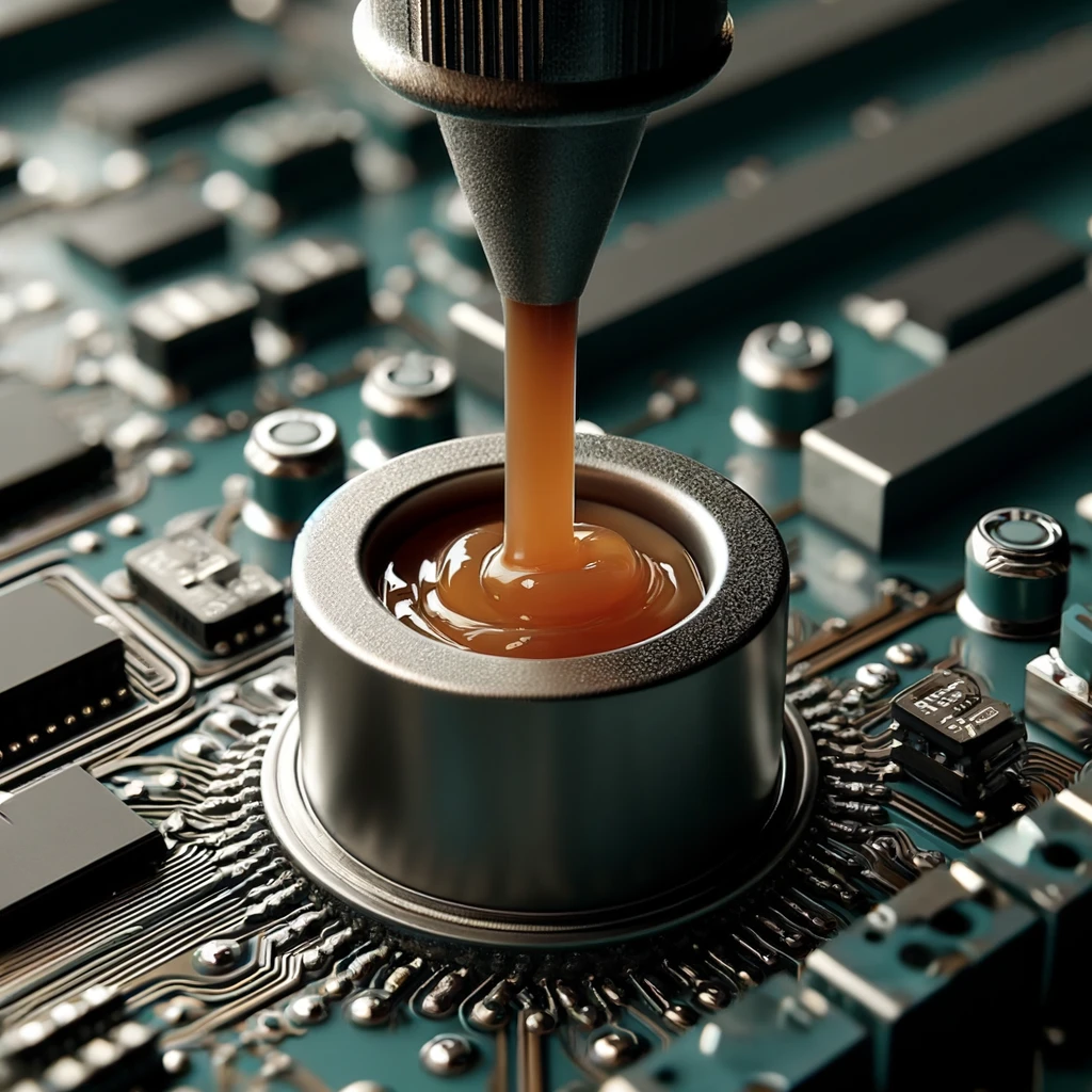
Non conductive via filling includes the process that the via fill holes in a Printed Circuit Board (PCB) with a non-conductive material like epoxy resin for non conductive epoxy material or non conductive paste. Here, the vias go through a series of chemicals to protect them from different atmospheric elements and to increase the ability of the board to withstand mechanical damage. However, those that are non-conducting are often employed when the appurtenance of electrical conductivity between two or more layers is unnecessary, or when the circuit’s division into isolated parts is required for instance, non conductive epoxy paste.
Copper plating shut filled vias
Copper filling via process is when copper metal is dropped to fill vias that appear in a circuit of a PCB manufacturing technique. The deposition of copper relative to a copper- via hole is one of the process steps that utilizes electroplating technique. The copper, which rests inside the generated via holes, leads to a conductive path between layers of a PCB or internal layers. This technique is generally utilized to increase the electrical conductivity and as well as the mechanical strength of the vias, enabling more precise and durable connections among the components of a board in surrounding laminate. Likewise, Through filling the vias with copper plated hole, the PCB’s thermal dissipation ability will be enhanced also making it more suitable for applications thermal management is very important.
Best Practices for Optimal Via Filling
Delivering in the printed circuit boards (PCBs) full capacity through following of detailed rules and implementation of professional approach, is a task that demands precision and observance. Some key practices include:
Proper Via Design
Prepare clear rules about the optimal width of vias, their aspect ratio and their mounting for every operation. By following design rules provided by the PCB manufacturer, errors that could slow down or hold up its production at the fab can be avoided.
Cleanliness
Be sure to maintain the cleanliness of PCB and the via filling process by keeping free of contaminants prior and during the process. Contaminants can prevent from the filling materials being bonded and may cause a reduction of the via’s reliability.
Controlled Filling Process
Employ a regulated process for stuffing vias that will ensure even distribution and prevent overfilling or deficit filling. From us: Implement a controlled vias stuffing process, which ensures level distribution of the material and prevents overfilling or deficit filling. Follow the guidelines while applying the recommended fillers and also monitor their curing properly.
Quality Control
Conduct full examinations and test to confirm the holes are properly filled into their right specifications. Utilize methods like cross-sectional analysis and electrical testing so that the viability of vias to be filled is verified.
Material Compatibility
In this regards, make sure the filling material remains compatible with PCB substrate and with the materials that are being used in the board. Think of the core factors like the expansion and contraction which can result into delamination or crack.
Consider Environmental Factors
Environmental factors such as temperature, humidity, and what is around them are all important things to think about when choosing a filling material. Select a material that can endure and has a good working life in these conditions.
Documentation
Proper documenting of every step of the fill lab process is a must, composing of the materials used, method parameters, and test results. This knowledge may be useful for monitoring and control activities to ensure certain product quality.
Through compliance with those guidelines, manufacturers are able to ensure correctness of vias filling process and their meeting all functional performance standards, which is resulting in high-quality and reliable PCBs.
What is the purpose of via filling?
To accomplish the goal in these situations, you need to make the raw materials more productive, obtain the best utilization of labor and capital and ensure a first-class quality of finished product and on times service. For the vias either wtih a conductive or non-conductive material such as epoxy resin or copper will be filled, thus improving the performance of the board by decreasing the probability of line slos and failure. Moreover, with thermosetting or compression molding, the strength of the board can be improved. This process can result in a panel that doesn’t crack or bend easily or that is more vibration-resistant. The last stage in PCBCs manufacturing process by filling is a critical step that helps in preserving the continuity and functionality of the board under different working conditions.
4 factors that affect the filling vias cost?
Though many contributions make PCB vias filling cost vary, several of them could be explained. These include:
Via Size and Density
Finer vias or higher-density designs entail filling dielectrics through increasingly precise methods necessitating materials that are of high quality and might be more expensive, thereby increasing the cost.
Filling Material
Cost of the filling material that is a part of the microvias can be also high. Properties electrical conductivity allows such materials as copper epoxy filled to cost more than those properties non conducting, such as epoxy resin.
Manufacturing Process
The manufacturing complexity can be a complicating factor from the costs perspective. The method which involves the use of high-end equipment or more than one steps of the process, for instance, electroplating, is very likely to be costly than other types that are simpler, like filling.
Quality Requirements
During this process both high ratios of quality of the product, such as tight tolerance or specific performance crafts, may also influence the cost. Getting these NC requirements may ask for more precise filling techniques or better grades of the filler, this is why the cost will rise.
What are the types of paste?
There are several types of paste used in various applications, including:
Solder Paste
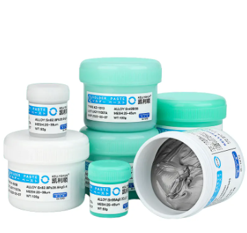
Applied in the automation of electronics assembly to fuse parts onto printed circuit boards (PCBs). The solder is in the form of solder alloy powder that well blenders with the flux vehicle.
Conductive Paste
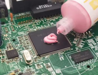
Has materials that are conductive that may be silver, copper or graphite, and is used to make electrical connections or in repairing broken traces on printed circuit boards.
Thermal Paste
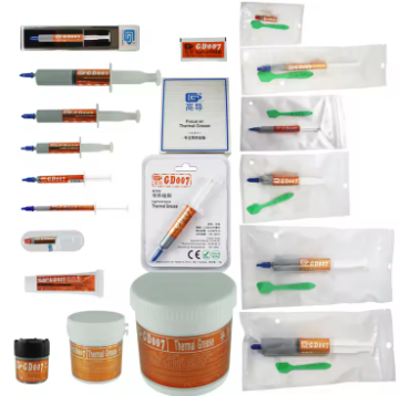
The role of thermal paste or thermal grease (thermal grease or thermal compound) is to increase the thermal conductivity between components that generate heat and electrical signals (like CPU and GPU) and the heat sink.
Adhesive Paste
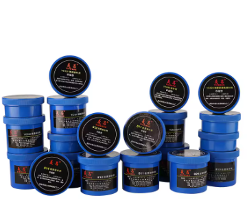
Used for bonding materials together, generally in assembly as may often happen in construction, or manufacture of heavy industries. A number of raw materials can be used which includes epoxy, polyurethane or silicone.
Dielectric Paste
A variety of applications in electronics is one of the major sectors in which cemented carbide are used for insulation or protection. It is insulation and is commonly chosen to package or to tin devices.
Types of Filled vias (Thermal conductivity and Electrical conductivity)
PCBs with copper-filled vias are more beneficial than boards with copper-plated vias in the following aspects:
- Thermal conductivity: Plating the via with copper leads to enhanced heat transfer route. By surrounding the board with the shield, the fill wicks heat will be kept at bay and the longer life of the unit will be achieved and defects that occur in applications where high heat level is necessary will not be affected. The dissipated heat from the microchips is conducted away from these vital components by copper and thermal expansion. This is due to copper`s high thermal conductivity. The heat flow does not permeate all around the copper board but from its one side to the other than to completely spread out at different spots of thermal transfer properties.
- Electrical conductivity: Credited to tiny vias which yield high currents, the copper-filled vias can be applied in cases where the power may need to move from one side of the board to another. A copper layer without heavy loading on the PCB can carry the large currents flowing from the inside thanks to copper’s conductivity. This capability is the main reason why designers feel the need to place in the design several copper-filled vias for PCB boards where the voltages are subject to be high. Hence, the standard byline reads that they are usually the most preferred in the fabrication of high voltage PCBs.
What are the advantages and Disadvantages of via filling plug with LPI solder mask
Advantages of Via Filling Plug with LPI Solder Mask:
- Cost-Effective: LPI (Liquid Photo-Imageable) solder mask, which is well-priced, is another feature of cost-cutting for via filling.
- Simplifies PCB Design: Implementing the LPI solder mask for via filling not only relieves, but also eases the PCB design procedures since the components are simplified and the amount of materials and processes needed is reduced.
- Enhanced Electrical Performance: LPI solder mask is a conductor of excellent insulation which in the end improves the whole electronics performance on the PCB.
- Environmental Protection: Vias that are fully filled with low profile insulative solvent coating will be more survivable in a harsh environment such as moisture and contaminants, therefore, increasing the board effectiveness.
Disadvantages of Via Filling Plug with LPI Solder Mask
- Limited Thickness: Large vias and vias with high aspect ratios are not seamlessly filled by LPI solder mask because of the marked limitation in its thickness.
- Mechanical Strength: In this case, the lapilli solder mask may not offer prescribed mechanical support like other filling materials, thus making boards fragile mechanically solder bridging.
- Processing Time: LPI filler mask for vias, added time to the whole process of board making may slow down especially for the boards with a massive number of vias.
- Compatibility: Figuring out of the LPI solder joints resistance, not all of the PCB materials and processes may be genocidal and because of this, it is limited in its application to specific instances.
IPC 4761 standards for via filling and via covering
IPC-4611, or IPC-461, is the name for filling and plugging PCB vias processes that is covered in its stand. These steps are important and unlike to interfere with the consistent performance of the PCB. Here’s a brief overview of the via in pad covering and filling benchmarks as depicted in the IPC 461 standards:
Via Filling
IPC-461 regulates the use of either conductive or non-conductive materials in the vias filling process or via in pad process. The standard particularize the standard method for filling vias e.g. via tenting, via plugging or non-conductive or conductive material through vias filling. The bypass quality is also mentioned, emphasizing on the criteria for evaluating its quality, which should not have voids, be full, and adhere to the via walls.
Via Covering
IPC-461 insures the accuracy of the vias processing which includes their coverage with the conductive or non-conductive materials. The standard is a guideline of the allowable techniques of covering vias application: solder mask, conductive paste and non-conductive elastic materials. Via via covering, on the other hand, is also necessary the quality is the evaluation criteria, which include coverage completeness, adhesion, and deficiency.
In the summary, IPC-461 refers to the suitable procedure through which the dependability and proficiency of the connection vias can be attained by clearly defining the necessary materials for filling and covering the vias by conductive or non-conductive substances. Laying down compliance rules ensure PCB manufacturers and assemblers produce excellent PCBs that are okay for different industries and applications.
How do you fill vias during PCB manufacturing?
During the PCB board manufacturing process, vias are usually filled the use of a process called via filling or via plugging This process becomes an application of a conductive or non-conductive material onto vias to fill the openings and the vias themselves so as to avoid the chances of a conduction error. Filled after a dispensing process – in which, we apply the material into the via and then cure it to turn it into a solid plug.
Filled Vias Manufacturing Process
The process of filling vias during PCB manufacturing involves several steps:
- Preparation: The dashed lines shown on the PCB are the vias and they have been mechanically drilled in or laser-drilled hole or hole depth by the manufacturer in its initial manufacturing process.
- Cleaning: A PCB is processed to remove any waste or contaminants through the sectional holes.
- Surface Preparation: Surface of PCB even via holes are prepaired in order to ensure the attachment of filling material.
- Filling Material Application: Fill material which can be metalized or nonmetallic is deposited into via holes. Such agents can be employed by a mix of techniques: screen printing, dispensing or plating among them.
- Curing: The filling material is cured, The filling material is solidified, usually through heat or UV light, to become a firm and strong plug in via holes.
- Planarization: Following the curing, the surface of the PCB is turned into a planiform plane by removing all the excess filling material and obtaining a leveled surface.
- Testing: The plated through holes, after they were populated with the necessary vias, were tested to ensure that conductivity and insulation were achieved at the expected level.
- Final Inspection: The PCB goes on the final visual inspection to verify thrus that the filled vias are fine.
The manufacturer can accomplish this goal by adhering to the steps provided earlier in the thread and ensuring that proper filling of the vias in the PCB lead to the desired optimal performance and reliability while strengthening pad attachment.
