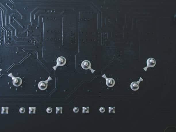
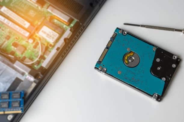
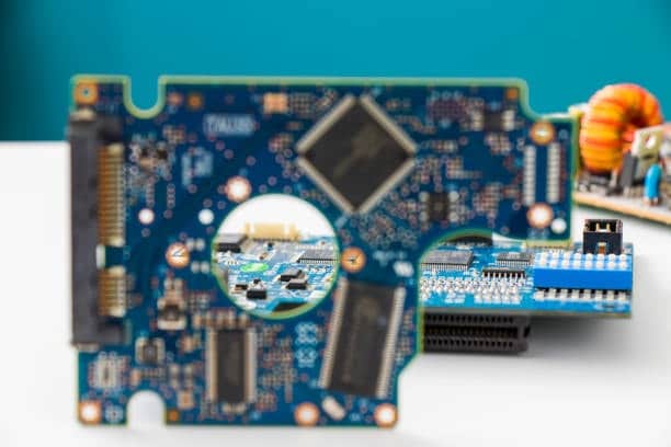
The lamination of PCB lamination is the most important procedure during production of printed circuit boards (PCBs), after which several layers are combined into an integrated one board. This way is known for the mechanical capabilities, strength, as well as operation of the PCB while it is being applied.
We will do an overview on the various lamination techniques, their benefits, advantages and best practices for achieving high quality results in this detailed guide we focus on professional printed circuit lamination.
Understanding PCB lamination process
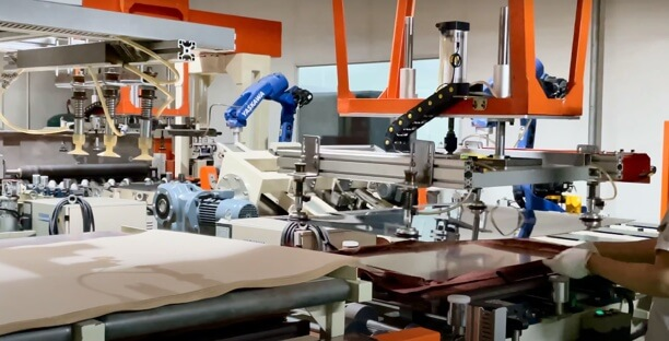
PCB Lamination process of laminating PCB layers PCB lamination which is the process of permanently binding the layers of multi layer PCBs created stacks up under heat and pressure and this entails bonding of multiple layers such as copper layerand the substrate materials using heat, pressure, and adhesive. The primary excellence which is needed to be achieved is the joint between layers with enough strength and reliability to keep unaltered the wire connections. The lamination process is hence an important factor especially for the PCBs intended originally for long-term use for the entire lamination process involves into the pcb manufacturing process also consists of placing the internal layers.
What is Sequential lamination process?
The sequential lamination process in PCB manufacturing goes laminating each layer of the circuit individually one by one also In this kind of sequential lamination technology process it would help to build up those layers of the board one at a time so in this kind of process is already done it by adding those layers and curing of dielectric material. The method gives you a greater control and precision concerning the alignment and positioning of the layers, especially shouldered by the complex designs which demand a precise charging of the layers with specific requirements .
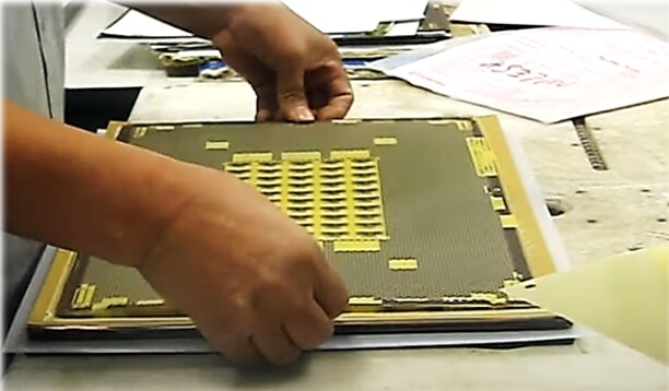
Every layer added sequentially, with careful attention to alignment to avoid misalignment issues, well taking into account the sense of alignment, so as to avoid the angles that does not give a complete sense of solidity. Although this method results in exact figures, a time-consuming lamination operation is needed which is typical for the standard printing circuits.
What are the types of pcb lamination?
The following is an infographic that illustrates the many forms of PCB lamination cycles:
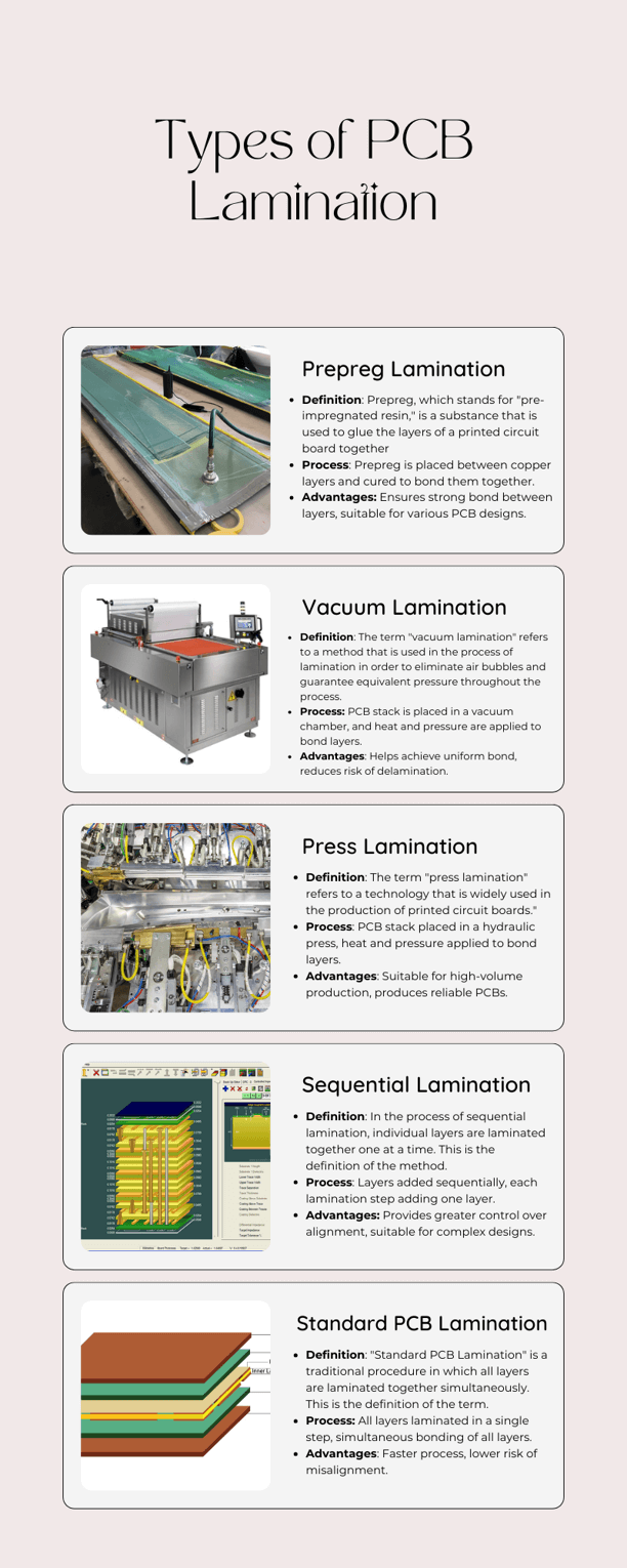
Prepreg lamination requires using a fabric called pre-preg, which is essentially a cloth with fabric and resin that is already in place. This is done by sandwiching this material between two layers of copper which are then put under a simmering temperature and pressure so as to fuse the two layers.
Vacuum lamination a technique which helps in evacuation of air bubble and provides uniform pressure during the lamination process. The sequential PCB stack is injected into a special chamber using vacuum and heat and pressure are applied to weld the layers permanently.
Press lamination Furthermore, another commonly used technique is press lamination where a stiller with the heat and pressure applied onto the PCB stack is used to bond the layers.
Sequential lamination, which involves laminating individual layers sequentially one after the other allows for more high level of precision and it fits best where stacks are complex using the sequential lamination technology.
Finally, standard PCB lamination is theis the traditional pcbs method which all layers laminate at the same level and turn to offer the faster procedure and reduced risk of click. Every lamination characteristic that is available comes with benefits and is selected based on the particular needs of a PCB layout and customization process.
Why is PCB lamination lamination is important?
PCB lamination is a critical production stage of PCB and hardware operation because it is essential for unifying mechanical structure of the circuit board and for making the circuit board of high quality and high-reliability hardware. The process of lamination, used in production, enables to bind together the elements of printed circuit board (PCB). This multi layer pcbs laminate system is composed of many different layers of prepreg (pre-impregnated resin,), copper, and substrates.
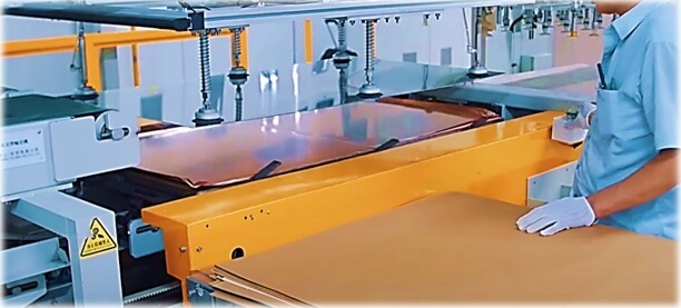
Besides being strength structure, which cannot exist without the interface between the layers, this process also makes the electrical connections between the layers, thus allowing the printed circuit board to exactly perform the function it was designed to be. It is very likely that lamination of a printed circuit board(PCB) contribute to its protection from different factors like dust and moisture since both these factors have the potential to affect the performance of the PCB fabrication if they are not carefully considered. Also for three lamination cycles, Just like the first cycle which are came from the layers 3 to 6 and then for the second cycle which came from the layers two and seven and then for the last cycle is came from the 1 to 8 PCB stack-up which are contains the called blind vias from 1-2 and then 15 to 16 there are the lamination cycle. In brief, the process of lamination of the printed circuit board (PCB) is a crucial stage in the PCB production. It is indispensable for ensuring that the boards are sturdy, durable and meet the new stringent demands of nowadays electronics.
What are types of PCB Lamination Materials?
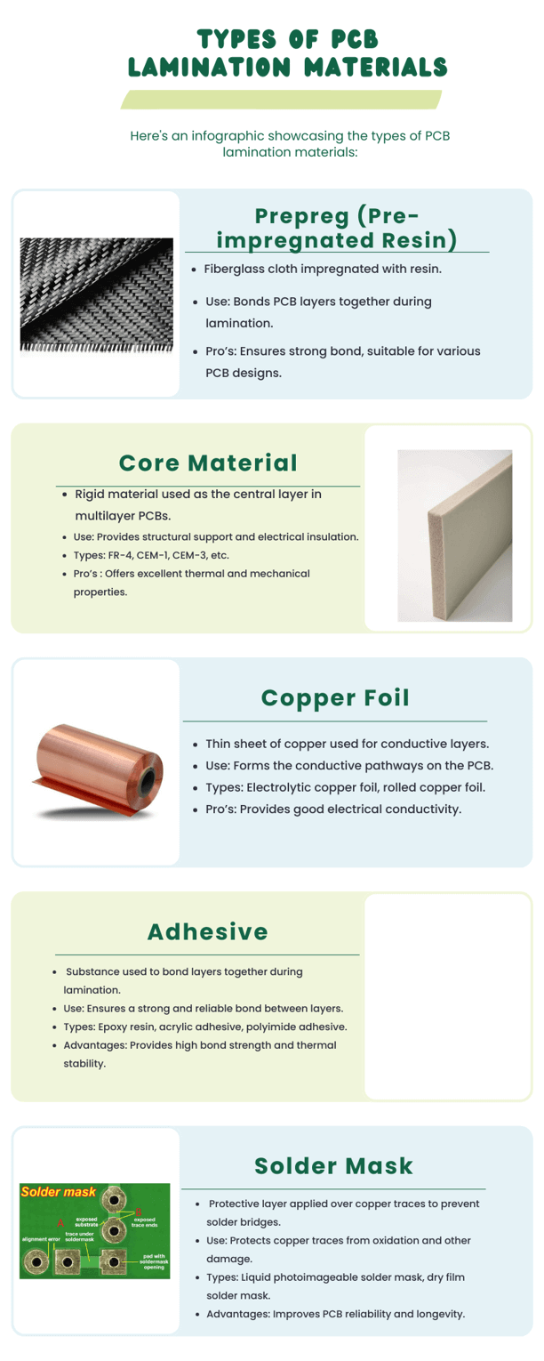
Prepreg (Pre-impregnated Resin) – As for the purpose of bonding double-sided PCB layer during the lamination process, prepreg material is fiber glass epoxy base material fabric that is applied with resin. In general, Composites meals a wide variety of patterns of PCBs for solid, high-quality bonding.
Core Material – When it refers to the multilevel PCB, this is the hard material at the center of the core layer, which performs the function of both electrical insulation of the PCB and as the structural support. Among many types, these can be found in FR4, CEM1, and CEM3, which are distinguished by their outstanding performance in heat and mechanical parameters.
Copper Foil – Printed circuit boards (PCBs) are a copper foil-based conductive path on to which a lucrative data transmission can be done and which provides outstanding electrical conductivity.
Adhesive – This type of material is used through the lamination process in order to provide the connection between the layers with a tendency to strength and durability. So you have epoxy resin, acrylic adhesive, and polyimide adhesive among types that are created to give strong bond strength between materials and remain stable at high temperatures especially during manufacturing.
Solder Mask – Solder mask becomes an excellent barrier when applied over copper trace layers as this prevents against oxidation and corrosion which results in better board life of printed circuit boards (PCBs)
What are the process of FPC Typical Production process?
The typical production process for Flexible Printed Circuits (FPCs) involves several key steps:
- Design and Layout – Ensure the circuit layout dimension is according to the characteristics parameters provided.
- Base Material Preparation – Flexible base material such as PI or PET is the usual preparation procedure – which can be a path to fabricating the necessary material. We can now go to the second step that involves the preparation of the material.
- Copper Cladding – It is a way of advertising the application of a thin layer of copper on either one or both sides of the base material in the copper cladding procedure. Carbon can be removed from the air by the process called as electroplating which is a common method nowadays.
- Photoresist Application – One of the processes in the photoresist application involves doping a layer building of photoresist over the copper-clad material.
- Exposure and Development – By using a mask to cover the photoresist, you can select the part of the circuit to be developed by UV Light irradiation. The copper that is covered by the photoresist is washed away to reveal it. So after the development process the photoresist is exposed.
- Etching – Clean the etchant up in the same process, as it is used in order to wash away the exposed copper layer, which leaves the traces of circuit footprint or to the thin etched boards.
- Stripping – Photodevelop expression of the rest photoresist from the top of the copper tracks, thus leading you to the the stripping stage.
- Surface Finishing –It is required that the copper tracks be enriched on the surface with coverings that would prevent oxidation of the copper metal and as well as to get the tracks soldered easily. These treatments which include HASL (Hot Air Solder Leveling) and ENIG (Electroless Nickel Immersion Gold) are widely adopted in practice.
- Solder Mask Application –Layer solder mask on the copper traces, keeping in mind the places where components will be soldered, on top of the solder mask. This is the ninth and last step involving the high frequency applications of the solder mask.
- Silkscreen Printing –A way to improve this product is by coming up with component designators, logos, and other related details while printing them on the board using the silkscreen method of printing process.
- Final Inspection – The final time of 11th and final check, the FCS should be inspected for any flaws or problems that tend to hinder its work better compared with others.
- Testing – This step must be done to ensure that the FPC is electrically continuous and has the other needed parameters. It is the secondary stage for the medical device testing.
- Routing and Scoring- During the routing and sciving the field-programmable circuit board (FPC) in separate boards Either a routing or scorings can be done.
- Final Assembly – If any of the parts should turn out to be absent necessary ones, such as resistors, LEDs and connections, they should be installed.
- Packaging – Package the FPC for the client on the basis of the transportation type, use soft and protective packaging materials.
How to Laminate a PCB?
A laminated PCB consists of several materials arranged into one lap that is interconnected. For the lamination of a PCB, the following steps should be taken: the PCB layers are prepared (e.g. the copper layers and prepreg), with their substrates materials layered between them. See to it that the copper layers are spick and span and not contaminated with any soiling. Then, stack the layers in turns starting from the back with the copper layer between septapreg and the substrate material. Next, assemble the stack in a lamination press and press it down with heat and a location for it to be placed. It generates the activating heat through the resin in the prepreg; thus, both of the layers get bonded together. Permit the stack to cool and solidify so as to ensure that the bond layers is complete. Let the stack to cool and cure to make sure that the bonding happens properly. Finishing touches are the last thing to be performed, which means checking the PCB for any defects as well as the processes like drilling holes or applying surface finishes. A successful lamination process would require proper positioning and temperature setting is an equally vital factors.
What are some common issues in PCB lamination?
It should never be forgotten that the numerous problems that may appear during the lamination of a PCB would result in poor quality with poor performance of the end product. Delamination, where layers separate processes within a PCB resulting in malfunctioning of electrical connections, is one of the problems in PCB. This may be due to insufficient resilience, fluctuations of lamination temperature and pressure, or material contamination for instance. The skill of the fabricator also determine the level of misalignment of the layers. This can be open or short circuits in the PCB. Incomplete lamination processed at low quality can result in PCB lamination void or blisters when the actual PCB is made which could further affect its structural strength. In addition to PCB stack temperature, warping and uneven bonding process on the other hand can occur due to overheating or underheating issues. Good process control and quality assurance measures are indispensable to overcome the aforementioned common issues and manufacture the surface boards of maximum quality.
How Does the PCB Lamination Process Work?
The passing lamination process of PCBs corresponds to gluing together several layers of materials so as to produce an entire circuit board. First and most, the preparation of the layers including copper layers, the substrate and pre-impregnated resin materials is manufactured. The following step puts together the inner layers in the specified sequence, with the outermost layer being a prepreg layer. Then the stack is squeezed in a lamination press, that uses the heat and pressure. The fact that resin from the epoxy prepreg is heated causes the layers to fuse together. Lastly, laminate is cooled down and is cured, the adhesion and debonding is complete. The PCB is done and this is followed by verification of quality plus any additional processes and then it will be used in electronic devices or appliances.
Conclusion
In the electronics field, the assembly of electronics PCB (Printed Circuit Boards) is a crucial process that ensures the optimum reliability and performance of electronic devices produced on a mass-scale basis. Through adhesion of these layers, for instance, copper sheets, substrate, and the pre ply of materials, PCB (printed circuit board) lamination provides integrity for the structural stability and durability. Such precautions not only increase the board’s durability to adverse conditions either in a high density interconnects or have high quality materials, but also, they are indispensable processes that reassure clear signal conduction and the absence of electrical obstacles also in laminating PTFE laminates. With technology moving ahead continuously, and the increasing complexity of electronic parts, lamination of PCBs stands out as a key activity in assuring quality operation and durability of the devices using those various layers.
