In these days, with the constantly changing technological industry, accuracy in the design of the printed circuit board (PCB) is a vital point. To a great extent, trace width management in PCB design is one of the key matters. This is an article that reveals new improvements and approaches in PCB trace width goal-setting for the designers to acquire more advanced board functions and resistance.
What Is a Trace?
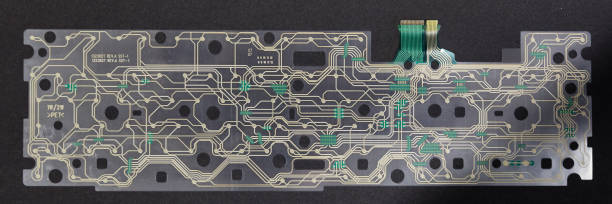
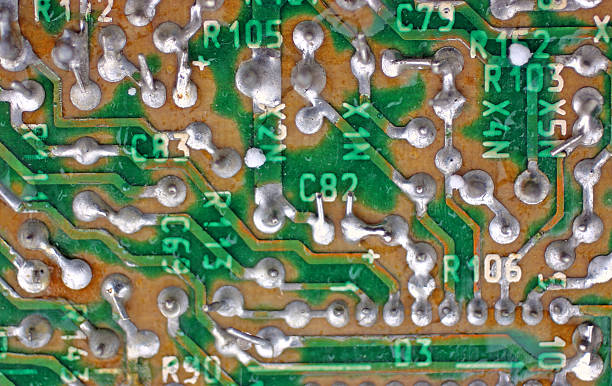
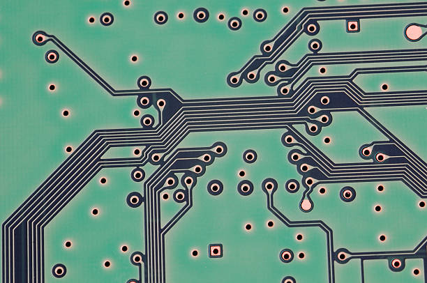
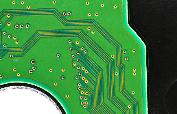
PCB traces are a fine copper-weight pathway that is manufactured onto a PCB by means of a process of etching that connects and links the different components, thus creating its network and allowing the electrical signals to flow throughout.
Why Trace Width Matters
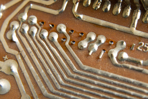
It was measured in mills, or thousands of an inch. While the standard trace width for these ordinary traces has no special requirements, it may be in the 7–12 mil range. The trace width is another vital factor in the design of printed circuit boards (PCBs), which contributes to the electrical interaction as well as the thermal characteristics of the circuit. Here’s why trace width matters:
- Current Capacity: Trace width identifies the amount of current flow through the circuit before the heat up begins in an excessive way.
- Signal Integrity: A suitable trace width helps signals nearer to punch through and reduces cross-talk with adjacent traces. This way, the signal fidelity of high-speed circuits is ensured.
- Durability: The circuit board design will dictate trace width and spacing, which determine the reliability and durability of the PCB, which will make it less susceptible to failure due to stress.
- Heat Dissipation: Higher traction lines dispel heat more gently because of larger surface areas. That is most significant, particularly for high-power systems, since high heat is hazardous rather than beneficial to the electronics.
Latest Techniques and Materials of PCB trace width
Continuous improvements in PCB materials and manufacturing technologies have become key for electronic design engineers who can choose the trace width as per the design. Here are some of the latest trends:
Improved Materials
In the modern-day board design of aircraft, high-performance materials such as High-Tg FR4 and polyimide provide trace widths that are narrow yet can withstand high temperatures. These materials are the best technology for placing chips on a small board, i.e., high-density interconnect technology.
HDI Technology
HDI technology allows such patterns like lines and spaces to be finer, thus, in turn, more compact and effective PCB layouts. These accomplish this by mounting advanced manufacturing processes like microvia technology that make it possible to manufacture miniatures packed with many traces.
Thermal Management Techniques
One of the developments in thermal management includes coin technologies, which operate from the inside surface of the package, and vias, which route heat from a hot die into a thermal path. These methodologies are very essential in order to sustain the functioning of the PCBs with trace widths that are under the microscopic area.
Calculating Optimal Trace Width
Among the factors to consider are the expected current load, the properties of the material, and the environmental conditions when calculating the width of a PCB trace. These tools, like PCB trace width calculators, can greatly help when simulating a printed circuit board with a cross-sectional area. They consider factors such as:
- Current Load: The trace will be subject to the maximum current expected to flow via it.
- Temperature Rise: The temperature rise definition (or the permissible increase in trace temperature) is given by the heat produced from the electric current flowing through the internal conductors.
- Copper Thickness: The variations in copper layer thickness within the line determine the current conduction, which is very crucial.
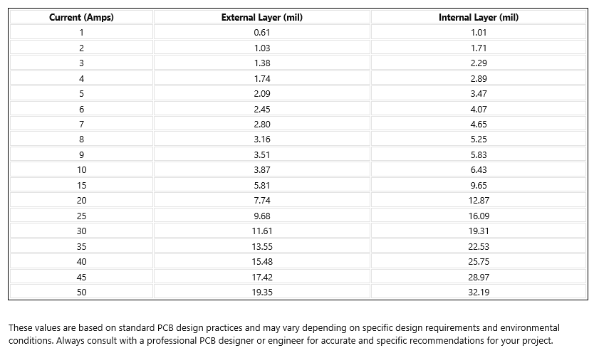
CHART IPC Recommend Track Width For 1 oz copper PCB and temperature rise to 10 °C
For the creation of a chart indicating the IPC recommended trace width for 1 Oz of copper traces PCB under a temperature increase of 10 °C, we would use the IPC-2221 guideline as a reference. These standards make a reference for unbound-line widths on the basis of both current-carrying capacity and temperatures rises. Below, I’ll provide a chart with typical current values and the corresponding recommended trace widths for a 1 oz copper layer, aiming for a temperature rise of 10°C to calculate trace width:
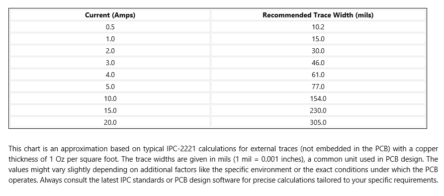
The table showing the maximum current carrying capacity (amps), minimum trace width for external layers (mil) and external traces, and minimum trace width for internal layers (internal trace widths) (mil) for 2 oz. copper with a temperature rise of 10 degrees Celsius of the trace thickness calculators:
Trace width-Related Specifications in PCB Fabrication
Details in the fashioning of traces are also among the major features of the PCB fabrication. The results of programs and the boards as well are another priority nature. Here are the essential points summarized:
- Trace Width and Spacing: Inerrability, capacity rating, and electromagnetic wave absorption are essential factors that should be taken into account in manufacture of solar panels such as the trace width and trace resistance. The carefully placed right line of the code stops the crosstalk and electrical circuit short at the same time.
- Copper Thickness: In majority cases, it is indicated in terms of ounces per square foot, and based on this assessment, the question is raised whether charges can flow effectively across such skin or not. A thinnest version of it weighs in at one ounce per square foot, or 2 oz for the thicker versions.
- Impedance Control: It is very significant to prevent the degradation of signals in such networks and this task is known as signal integrity The resistor value is controlled by trace width, substrate material and design configuration.
- Geometry: designed with few sharp turns; no crossing paths and isolated traces as much as possible for low impedance effects.
- Thermal Management: In intimate tracing design, you need to consider the heat dissipation and you could handle it with broader traces or thermal vias.
- Annular Rings and Pad Size: It is a fundamental thing and enables trustworthy contacts as well as good mechanical properties of the via and the component pad.
- Surface Finish: it becomes possible to choose variants based on solderability, stability to corrosion, and environment: such as HASL, ENIG, and OSP.
- Etching tolerances: The etching process is particularly important in as far as tight trace widths and spacing are concerned and this makes it the only decisive factor since the detailed circuitry is the main contributors.
- Repair and Modification: Do not restrict the specification to the parameters that will be machined before delivery, but also allow later potential mending of irregularities.
- Durability: Paths to be built should be designed to withstand environmental and mechanical stresses, particularly on flexible PCBs and their hybrid versions.
These requirements are basic and essential for designing and manufacturing the PCBs that function as per the provided conditions of the operations without suffering any adverse effects.
What Factors Are Essential for Trace Width?
When determining trace width in PCB design, several essential factors must be considered to ensure functionality and reliability:
The table listed below already gives a decent illustration of the components that should be balanced to attain optimized PCB performance and reliability.
- Current Carrying Capacity
- Temperature Rise
- Impedance Matching
- Voltage Drop
- Manufacturability
- Space Constraints
- Thermal Management
With the aforementioned table, this section clearly shows a number of factors that must be considered when adjusting the trace width, so the PCB circuit can work effectively as well as reliably.
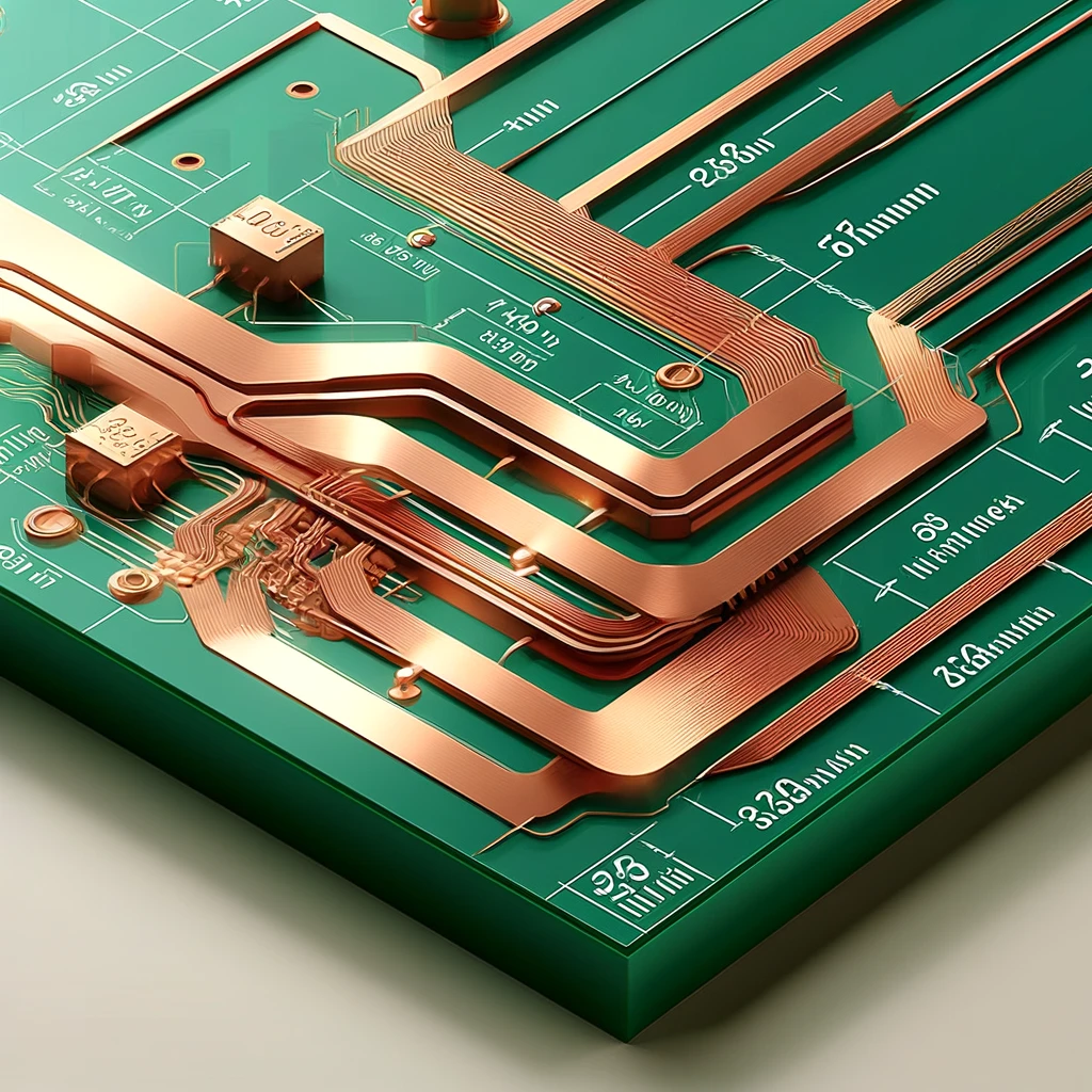
Various Trace Widths and Thicknesses (clear picture)
To provide a structured and clear representation of various trace widths and thicknesses used in PCB design, here’s a table that shows common values and their typical applications:
- Trace Width: On the opposite side of the print, this is the width of the copper trace. This essentially implies a reduction in the electric current conduction ability and impedance that the trace mostly experiences. Wider change ways conduct higher current limits and ease heatiness. A number of trace widths are generally used for PCB designs, which broaden out from a couple of mils (thousandths of an inch) for low-current applications to wider ones for high-current applications.
- Trace Thickness: Here, the copper trace follows a cup-like structure. It is usually expressed in ounces per trajectory; this literally translates into a real thickness in milter. Standard copper thicknesses are:
- 1 oz/ft2 = 1.4 mils (about 35 microns)
- 2 oz/ft2 = 2.8 mils (about 70 microns)
- 3 oz/ft2 = 4.2 mils (about 105 microns)
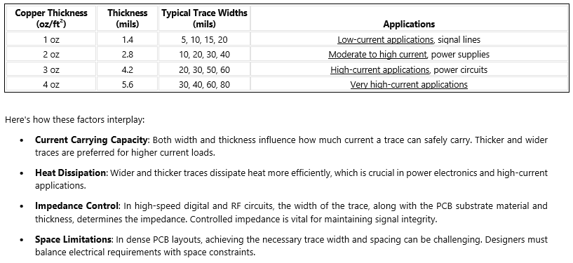
Key Points:
- Thickness (mils): These cells are the thickness of copper. Each square foot of copper equals about 1.4 mils (or 35 microns) per ounce of thickness.
- Typical Trace Widths (mils): Here is an example of copper conductivity values that show common trace widths you could use for different copper thicknesses. The thicker the traces, these are the structures usually made of copper to cope with an increase in current and conduct heat generation.
- Applications: This is the column where the outline of the typical applications for every range of trace width and copper coating thickness is given, enabling designers to make the right selection of the pin width and coating thickness based on the electrical specifications of the PCB.
Trace Width and Signal Reflection
In digital PCB design, signal reflection is greatly dependent on trace width, especially where high-speed signals need a smooth transition from one node to another. Line-trace width impacts thermal impedance. In cases of improper impedance matching, signal reflections will take place, which negatively affect signal quality and data integrity. One of the methods to reduce reflections is to make the source impedance of the antenna match the connected components and the source impedance, usually 50 or 75 ohms.
Reduction in trace width is the customary way to meet impedance matching objectives. Trace widths with higher impedance are typically lower traces, while narrower traces raise the impedance and trace cross sectional area. A wide spectrum of electronic design software could be used for that purpose in PCB design to run simulations for optimal trace width, thus achieving controlled impedance and reflected signal minimization. The proper trace design, which incorporates consistent widths and automated routing as well as correct termination techniques, allows for high signal performance in complex electronic systems.
Best Practices for Trace Width Design
To master PCB trace width design, follow these best practices:
- Use up-to-date software tools: Make use of the latest PCB design software, which has attributes like auto-routing and trace parameter fitting with the help of constraints due to electrical parameters and thermal constraints.
- Regularly Update Your Knowledge: Obtain new materials and technologies related to the trace width adjustment process.
- Consider Future Modifications: Consider things that may become upgrades in the future during the design process. Having accommodation for wider traces where possible would allow for the power demands as well as changes in the specifications of the components to be thwarted.
PCB Trace Width Calculator Input Data
Giving exact data as input when using a PCB trace width calculator is the basic principle to follow to get trace width size computations by the calculator, to be precise. Here’s a table that includes typical data values and explanations for each parameter necessary for the calculation:
Example inputs for calculation:
- Current Load: 2A
- Copper Thickness: 1 oz
- Temperature Rise: 10°C
- Ambient Temperature: 25°C
- Trace Type: External layers
These multiple inputs make sure that the track width of the track is neither large nor small to the extent that the PCB board process all the functions safely during unfavorable condition, able to resist electrical load, lowering the need for temperature control mechanism against high temperature.
Conclusion
The key to my accomplishment in electronic product design is making the trace width a manufacturing success, which has the result of using products that internal traces are highly efficient and highly reliable. On the other hand, designers can be more competent in their PCB by knowing the newest material, latest technology, and How to calculate it technically. This is how they can perform their PCB task with high accuracy. In the global technological theatre, your very important tactic might be continuous learning by constantly utilizing new technical improvement and elaboration in printed board designing.


