On circuit board the tracks connect to form a network of electrical routes linking the components in a specific geometry. The component interaction from one to another and the way in which the flow of electrical pulses through the board are both defined by this design.
What is circuit boards?
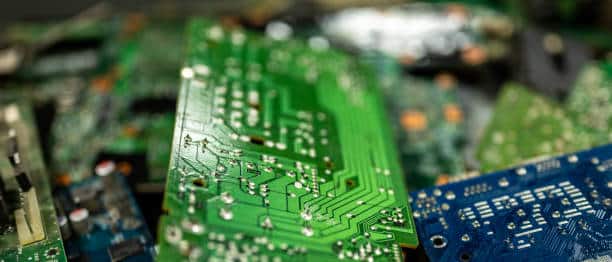
Printed circuit boards (most often abbreviated as PCBs) are indispensable in contemporary electronic devices. As are circuit boards sometimes called PCBs. It is a medium where the different electrical components, such as resistors, capacitors and integrated circuits are joined together and held together. The board, in turn, consists of a non-conductive material, mainly fiberglass. More complex than it appears, this process involves non-conductive material that has been coated with tiny layers of conductive material, which are commonly made of copper, being etched on the board to create pathways that allow electricity to pass through and which connect all of the parts that are included on the PCB board.
Unlike the general cable pathway systems, these paths are configured through the utilization of specialized software and manufacture techniques that lead to the right placement and routing of connections. Boards for circuit are very important elements of the processes that make electronic systems from complex components orderly and structured. They are among the factors that ensure smoother communication and operations in the world of devises, which cover cellphones, computers, industrial machines, and spacecrafts among others.
History of circuit boards
The history of electronic circuit boards begins at the dawn of the 20th century and is linked to the evolution of radio technology. Point-to-point wiring was used to construct the early circuits, which was very tiring and full of mistakes.
It was during the World War II that the advances in electronics led to the creation of the first true printed circuit boards (PCBs). These PCBs relied on copper tracks printed on a non-conductive substrate to connect the components. Starting from the latter half of the 20th century, the PCB manufacturing processes continued to develop significantly due to the improvements such as the automated assembly techniques, the surface-mount technology and the miniaturization.
These innovations have changed the electronics market, currently allowing manufacturers to produce smaller, cheaper and more reliable electronic devices. The ubiquity of the circuit boards cannot be underestimated, as they are now indispensable in almost all electronics from gadgets to medical and aerospace applications as we progress technologically.
How do you make a circuit boards step by step?
For the creation of a circuit board, there are numerous essential steps:For the creation of a circuit board, there are numerous essential steps:
1. Design
The first stage of the process is to design the layout of the circuit board using the special programme. One of the processes involved in this is identifying the location of each component, traversing the connections, and keeping electrical integrity.
2. Substrate preparation
This procedure comprises the obtaining a non-conductive substrate material, commonly a fiberglass epoxy-laminate. This substrate will be used as underlayment for the PCB board some time later.
3. Copper clad laminate
The third option is both Laminated Copper Foil (LC) coupled, FCC as well as RH side of the substrate during the manufacturing process. This multiple layers of copper will function as the pathways that electrical currents will go through.
4. Photoresist applications
The forth step is coating substrate with the photoresist, which we do by coating copper surfaces with a photoresist layer. The photoresist layer will be used to protect the copper during the etch process and to ensure selective protection.
5. Exposure and Development
The printed-circuit design is transferred onto a transparent film which will then be aligned and exposed onto the copper surfaces covered with photoresist layer within the photophore after the printing stage either in the bare board. After that, the board is etched to get rid of any extra photoresist that might have adhered to the copper lines in an undesirable way. This will ensure that the board is patterned properly.
6. Etching
To remove the exposed copper areas which are not covered by photoresist, a chemical solution is needed during etching. What is included is the removing of all the copper areas which are not the traces that form the circuit pathways.
7. Drilling
In the process of drilling the holes are drilled into the local areas of the circuit board where the components are to be attached and the electrical connections are to be established (while the board is layered, for example).
8. Component leads placements
Given the circuit board layout, electronic components are assembled to the circuit board. It can be performed manually or with the aid of automatic assembly equipment to get this done.
9. Solder paste
The process of soldering refers to joining the components to the copper traces through wires, which act as the electrical connectors. Surface-mount components can be soldered for example with a reflow soldering oven, while through-hole components may be soldered either manually or wave soldering machines.
10. Testing and Inspection
The circuit board that is being built is subjected to testing to ascertain that it is working as required and that it does not get electrified. Visual inspection is also included for checking the faults or any other problems with soldering.
11. Finishing
In the process of finalization, the PCB may undergo some additional processes like coating it with protective solder mask and silk screening which is done for the purpose of labeling and component identification.
12. Final inspection and packaging
All the tests are passed and any modifications are made after they have been passed. Then the circuit boards are evaluated for the last time prior to being shipped or assembled into the electronic products.
What are circuit boards made of?
Circuit boards, which are often referred to as printed circuit boards (PCBs), are normally made up of a substrate material that is non-conductive usually in the electronic device. The most frequent combination of this substrate material is fiberglass-reinforced epoxy laminate.
When it comes to the electronics, this substrate serves as a solid foundation. After that, the substrate is laminated with thin layers of conductive material, which is often copper. This creates the circuit traces and pads that are used for soldering electronic components or electronic device. Etching and photolithography are both procedures that are used in conjunction with one another to create patterns on the conductive material for the electronic signals to have power and ground planes in some electronic component.
It is possible to apply additional materials, such as a solder mask and silkscreen, in order to protect the board and give labeling, respectively. Generally speaking, the combination of a substrate that is non-conductive with traces that are conductive makes it possible to create complicated electrical circuits in a form factor that is both small and dependable. This is a key feature for contemporary electronic devices.
How is printed circuit board work?
PCBs are also commonly referred to as printed circuit boards, which they use to interconnect and operate the electronic components within an electronic circuit They do this by establishing a platform to mediate them in top and bottom layers in the computer circuit boards. It begins with the designing of the circuit layout that comprises selecting of the component places and the electrical connections routing. Then the design is printed on substrates that are nonconductive like fiberglass reinforced epoxy laminates.
With the top of such substrate, thin sheets of conductor materials, usually copper, are laminated. The copper traces combine to form routines that help in the transmission of electrical impulses between components multi layer boards. It is calling the circuit finished when the components have been soldered onto the board. Thus, current can flow between the components and tracks that have connections.
One of the most effective solutions in the fabrication of modern electronic devices like phones, computers, medical equipment, and automotive systems, PCBs provide a method of structuring and arranging electrical circuits that is compact and reliable for electrical signals.
What is the connections of the PCB traces to component leads?
The soldering method is a typical way in which traces on a printed circuit board (PCB) and component leads are connected. The solder is a metal alloy. It is also referred to as solder. The solder is heated to its melting point and then applied to the join formed between the circuit board trace and the component lead with insulating material. The bond forms due to the process of cooling and solidifying the solder, which is solid as well as conductive. Hence, an acceptable and lasting electrical contact is created between the component lead and the trace to the electronic components mounted with own circuit boards and have conductive layers with entire board to the circuit board design in power supply.
The soldering of surface mount components using solder paste and reflow soldering methods is achieved by soldering them directly onto the traces of the printed circuit board (PCB) without leads, which are in essence metal pads. The process consists of warming up the whole board until the solder gets melted and connections are made. On the contrary, through-hole components have leads which inserted into the through holes which drilled on the printed circuit board (PCB).
The component and the leads are connected to the traces by soldering these on the other side of the board, which gives rise to the formation of the connections of the component just like electrical energy with thin layer, green solder mask, electronic switches. In most cases PCB assembly requires soldering as it provides reliable electrical interconnections between the components and the component board.
What are the eight types of PCB assembly?
The following are the eight different kinds of PCB assembly:The following are the eight different kinds of PCB assembly:
1. Surface mount technology
SMT is an assembly technique whereby the components are attached onto the surface of a printed circuit board that are made conductive by solder paste and reflow soldering.
2. Through hole components
For those components that are of through-hole type, it is convenient for leads to pass through the pre-drilled holes on the PCB. The leads have a strong mechanical support from these leads attachment which has been done on the other side of the board.
3. Mixed Technology Assembled board
It combines SMT and THT components on a PCB, thus providing more possibilities in the selection of components as well as the assembly procedure.
4. Ball Grid Array
Beyond-glass-array components are provided with an array of solder balls at the bottom of the package. These solder balls at the pads are the matched ones on a PCB.
5. Chip on boards work
one of the type of assemblies that involves soldering semiconductors directly on top of the PCB substrate and bonding them to the circuit traces using wire bonding.
6. Microelectronic Assembly
This kind of assembly involves putting constituent very small electronic elements on a printed circuit board (PCB) via particular methods. One example of this kind of component is the microchip, and the other one is the sensor.
7. Flexible PCB assembly
Putting Flexible PCBs into Practice Flexible printed circuit boards (PCBs) are manufactured using materials capable of stretching, making them adaptable to different shapes. Adhesive methods of mounting which is appropriate to flexible boards are used in the attaching of components to these boards.
8. Rigid- Flex PCB assembly
Rigid-flex PCBs refer to a type of the printed circuit board that integrates rigid and flexible substrates into one board. This process of interconnection is achieved in such a way.
Basic components of a circuit boards?
A circuit board is comprised of the following fundamental components:A circuit board is comprised of the following fundamental components:
- Resistors – Usually, these components are used for controlling voltage or to protect the other components and the electrical current is restricted by such components in a circuit.
- Capacitors – Capacitors are utilized in filtering, smoothing out voltage variations, and coupling signals in electronic circuits. They are permissive of the of storage and ejection of the electricity energy.
- Inductors store energy – are widely used in applications such as filtering, signal processing, and energy storage as current flows through them. Hence, the energy is stored in a magnetic field.
- Diodes – very widely used for rectification, voltage control, and signal demodulation. Diodes are defined by the fact that they may pass current passage only in one direction.
- Transistors – The main functions of transistors are signals amplification and switching, the transistors are the electronic devices. These devices are building blocks in digital and analog circuits. We must note that in this case a gate is a three terminal device.
- Integrated circuits – These components that are developed on a single chip are called integrated circuits (ICs). Different types of ICs can perform a range of tasks, such as amplification, signal processing, and logical operations.
- Connectors – Connections between the PCBA and external devices are establish through connectors, which furthermore bring about the interfaces and modular assembly. Connectors provide the means for making both mechanical and electrical connections.
- Switches – To control the current inside a circuit, switches are employed. Theses switches provide users not only with the opportunity to switch circuits on and off, but also to choose between several operational modes.
These elements together with copper traces on the printed circuit board (PCB) form the supporting structure of the electronics circuits, which in turn provides a groundwork for the diverse implementations of electronic products.
The design and layout of a circuit boards?
In the design and layout of a circuit boards work which are being involved in those several key steps which are:
- Schematic Design – is the process which entails the making of a diagram of the circuit by the engineers showing how the components in the circuit are linked with the functionalities of each component also noted in the diagram.
- Component selection – a result of the specifications of the components, the performance degree of the components, and the fit of the components with the application for which they are chosen.
- PCB layout – The schematic is next fed into a computerized software by engineers, which in turn produces the physical layout of the printed circuit board (PCB). This architecture is characterized by the positioning of parts and the wiring of lines.
- Placement – where the components of the printed circuit board (PCB) layout are aligned, observing multiple aspects including signal integrity, thermal management, and the eventual assembly.
- Routing – The electrical connections, or traces, are routed between the elements with regard to the design restrictions, such as the signal integrity, impedance control, and minimize the electromagnetic interference (EMI) with copper layer, wire connector lugs.
- Design Validation – To achieve the design specifications and requirements in terms of functionality, reliability, and compliance to design standards, the printed circuit board (PCB) design and layout goes through a rigorous review and validation process of simulation, analysis, and prototyping and other essential components with automatic optical inspection.
- Manufacturing process preparation – Upon the completion of the design, manufacturing files are developed. The files contain Gerber files for the fabrication of the printed circuit board (PCB) and directions for the assembly process of the circuit components positioning and soldering.
- Fabrication and assembly – After that, the files that contain the PCB design are sent to a fabrication facility, and its job is to fabricate the board that consists of activities, such as etching, drilling, and plating. Once the components have been assembled, they are then soldered on to the board using either a manual or automated assembly method.
- Testing and Iteration – assembled pcb it will goes for testing in order to verify the functionality and the performance so that those any concerns and issues to identify during the testing it may also required the design iteration and also the refinement.
What are traces in a circuit boards?
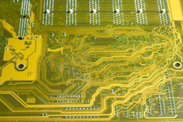
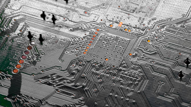
Traces are conduction paths, which can be found on a PCB(printed circuit board). They are the ones that carry out the transmission of electrical signals between any of the components and the different places within the circuit. Often copper is used to make these pathways, and their shapes are etched onto the surface of the non-conductive substrate material that is typically a fiberglass-reinforced epoxy.
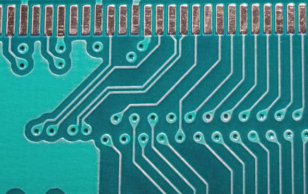
This material forms the base on which the printed circuit board (PCB) is built. There are various design requirements for the circuit that may lead to different widths, different thicknesses and different routing patterns for the traces. Sometimes, routes can also be different as well. The wires serve the purpose of connectors within the circuit, making a passage for electrons to travel between one component and another, thus facilitating the electronic device to achieve its tasks.
For traces to ensure a correct signal integrity, impedance, and electrical isolation, there hav e to be meticulous planning and routing. Besides, there are other factors that need to be taken into account which are, for example, the control of temperature and the minimization of electromagnetic interference (EMI).
As far as the operation and output of circuit boards are concerned, the trace is the one that determines everything. The traces are made to allow the electricity pulses to move in electronic devices.
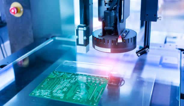
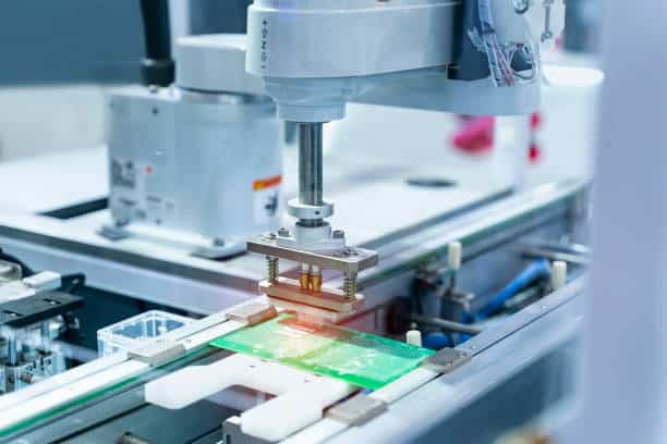
Process of circuit board fabrication
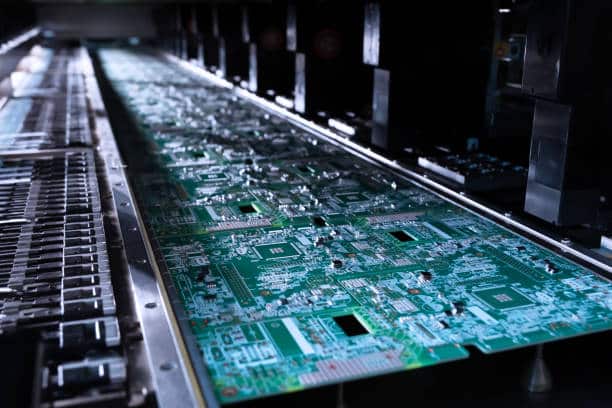
The circuit board manufacturing process is a step-by-step one, in which a design becomes a real board. Bonding thin strips of copper foil onto a substrate material which is typically a fiberglass-reinforced epoxy laminate, is done. The substrate material preparation starts the process. Then, the desired copper pattern is etched on to the substrate using photolithography processes.
After that, a routine is carried out drilling holes for the placement of components and vias for interlayer connection. In the next course of action, copper plating is used to provide electrical pathways between layers and surface finish is applied to keep copper from rusting and to make soldering easier.
This process starts by solder mask application over the board, which is then followed by silk screen printing. Then the planks pass through routing and profiling until they are fitted dimensionally, which is the stage following careful testing and inspection. Final circuit boards are then ready for component assembly, an important step for the device to have the ability to fulfill its intended purposes.
Digital electronic circuits and logic gates
Logic gates are indispensable structuring elements which are applied in digital electrical circuits. The presence of these gates is fundamental for their role of performing logic operations on binary inputs to produce binary outputs.
These gates, which include AND, OR, NOT, NAND, and NOR, each gate has a truth table that hooks up for it. Signals composed of 0s and 1s that represent binary digits are processed by these gates in these circuits with integrated circuit, pcb milling machine, molten solder. These signals are consequently modified to just perform some tasks such as addition calculations, data storing, and decision making.
This way, we can build digital systems, which are very complex, like microprocessors, memory units, and controllers replacing gates with various connections. The logic design and operation of digital circuits are based on precise combination of logic gates. The elements in these combinations allow them to process and store digital information and thus they are the heart of modern computers and electronics.
Functioning of a circuit boards work
The purpose of the routine of circuit boards is to serve as a platform where the components within an electrical circuit can have an easy connection and operation. The patterns in which the board is arranged, using non-conducting substrates with etched tracks, makes it simpler for the electricity to flow from one component to another.
The components, which are resistors, capacitors, transistors and integrated circuits, are soldered to the board upon the design that has been defined. The circuit generates energy, which results in energy flowing through the conductive pathways. This allows the components to cooperate with each other like a well-oiled machine and perform the tasks they are designed to perform.
The networked components perform logical processes, adapt, and perform actions based on the information entered into them. The efficiency of the electronic components is because the circuit board is well organized and contains the exact connections.
Therefore electronic devices ranging from the simplest calculator to the most complex computers and electronic systems can function reliably.
What are some common issues and troubleshooting?
Shorted pads, broken components, interconnect short circuits occur very frequently with PCBs. As such, orchestrating these complications may involve a strategic design. This type of strategy typically starts off with a visual inspection intended to look for any physical damage or incongruities.
The use of a multimeter to test the individual components may aid in deciding whether or not any of the component is bad. In addition to frequently using a power meter, an oscilloscope or signal tracer could also be of great help in locating areas that suffer from poor signal integrity or electrical noise. Open connections or short circuits can be found by checking the connectedness and insulating resistance.
If the problem continues to be the case, we may possibly need to do either better grounding and shielding or do a fault analysis on the circuit design and architecture to look for mistakes. Ultimately, there are elements of the diagnostic tools, technical expertise, and general implementation of the methodology of fault finding which are critical for the identification and addressing of problems of printed circuit boards.
What is the role of electricity in a circuit boards?
boards of circuit are key as electricity is the medium through which both signals and power get transmitted among electronic components. Hence, electricity is held as a significant feature of the circuit board. On switching on a circuit board, electrical current would pass through the conductive traces found on the circuit board.
By this relationships are being formed among different components of the system and they start doing the job that has been given to them specifically. Through the conveyance and control of signals like data transfer or voltage management together with the activation of electronic items like switchers and LEDs, this direction of electric current is made possible.
The circuit boards enable the functioning of the electronic devices – from basic switches to the sophisticated microprocessors – and power the current range of technologies from modern communications to computations and automatic systems. This is the way they achieve this by letting them pass through certain routes, planned beforehand.
Connection of PCBA traces to components
The contact of traces and components is considered as the main stage in PCBA that is a process that secure the functionality and reliability of electronic circuits with printed circuit boards. The soldering process is used to develop connections between components to the traces, which are conductive channels in the circuit board, the printed circuit board (PCB).
In the case of surface mount components, there are leads or pads which are soldered onto their matching copper traces on board surface. Mostly, such a procedure involves laying solder paste on the pads and setting the components on the paste and then heating the assembly in order to melt the solder, so obtaining a permanent and stable electrical connection.
Oppositely, through-hole components come with lugs that are poked into holes that have been dug on the printed circuit board (PCB). In the other side of the PCB, the leads of the components are soldered to the traces, which as a result of this operation, the connections of the components are formed. We need to be very careful to use the correct soldering process is to achieve qualitative solder joints and the reliability of the electrical connections.
Usually, adding connections from the traces to the components is among the vital steps in the process of printed circuit board assembly (PCBA). This part of the circuits would act as the channels of electromagnetic signal or power flow inside the electronic circuits.
The composition of the PCB board
The typical electronic circuit board, also referred to as printed circuit board (PCB), is usually made up of several layers of different materials that all complete each other to form to electrical circuits when put together semiconductor material and ground plane with various components. The major composite material tends to be an epoxy laminate with fiberglass as a reinforcing material that is used for the substrate how to circuit boards work.
The laminate is capable of giving both the mechanical strength and stability. This is then followed by the formation of the conductive pathways or bonds (traces) between the two sides of the substrate by bringing together thin layers of conductive material usually copper. Beneath the solder mask layer, bare board traces are coated. Components pads and vias are left intentionally uncovered. This will help prevent copper traces from oxidation and from deteriorating under the natural condition.
Also, in the sake of the component assembly easier, a surface finish, such as HASL (Hot Air Solder Leveling) or ENIG (Electroless Nickel Immersion Gold), may be applied on the exposed copper surfaces. Silkscreen printing is commonly utilized for the purpose of defining component outlines, printing part reference indicators, as well as additional labels. Finally, to put it all together, the PCB board is produced.
First and foremost, materials that have specific characteristics are joined. These features are represented by four aspects: conducting electricity, mechanical support, protection, and labeling that have to be known for the design and running of electronic circuits.
Conclusion
In essence, circuit boards are among the indispensable elements in the functioning of electronic devices because they provide the structural guidance for the connectivity and function of the electronic components with passive components or various components and have electromagnetic energy with double sided pcbs either two circuit boards. The circuit boards provide a passage for electricity and signals inside the electronic circuits by combining the conductive traces, resistors, diodes, capacitors, and insulation material. This makes job performance and operation of various tasks achievable that is why these are board controlled.
Modern technology advances in the range from a simple switch to a complex microprocessor and their presence on the circuit boards is now a necessity. The boards serve as the incubators for innovation and progress in the fields of communication, computer and automation. Restraints of scope and hardware limits necessitate the engineers and technicians to grasp the design, manufacturing, and assembly processes of circuit boards. In the end, the functioning of circuit boards is a clear indication of how they influence gadgets to provide for these needy gadgets we are almost stuck with in our daily lives.


