Let’s venture into the world of PCB designs with the guidance provided in this in-depth article. Starting from design of analytical sheet to the assembly phase or bare board, the process of constructing high-efficiency printed circuit boards involves several techniques to pcb design rules, pcb design tool, pcb outline. Whether you are a newbie or a technophilic or own pcb, this blog will prepare you with the know-how and skills to design PCBs with ease and elegance, and ultimately bring your ideas into reality with total precision and speed.
What is printed circuit board?
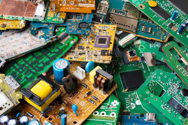
A printed circuit board (PCB) is somewhat convoluted comparing to an electronic hub. It plays the role of a connector inside the device that harmonizes all the electronic parts. Copper streaks (or sometimes copper traces) are the wiring that connects components and carries electrical signal(s), thus making a system function effectively. The substrate is the substrate of the board which is all the under-laying structure giving a stable base. As tiles and bricks are the main constituents of a house, resistors and capacitors are components which base it on. Solder mask duty shields used components from damage as well as many adverse factors. Lastly, silkscreen is imperative in case of security labels or printing information. And these characteristics are crucial for PCBs repairs because of it allows everyone uses PCBs smoothly.
What are the basic steps of pcb design?
The core pieces of PCB design include a number of stages which all are equally important for a circuit board which can really work good and have a solid efficiency. Here’s a simplified overview:
Schematic Design rules
That is the act of the schematic engineering which they do using the software that is specific to perform the task of determining the components connection of pcb rules.
Component Selection
Those are vital for PCB design and production, as well as the way their circuit boards work. They have to obtain the necessary components that will meet the design requirements, cost and availability of the components.
Board Layout Design rules
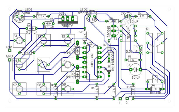
Components are laid on a jig called a board and traces are routed or trace width using copper consider schematic as an input. It is the step to represent the whole board layout design. This is the third stage in the board layout design process. In this phase, thorough analysis of various parameters, such as signals integrity or integrated circuits and thermal control, are conducted.
Gerber File Generation
The Gerber files form and those contains on which data is required for printed circuit boards manufacturing, for instance, board composition for instance, copper layers, solder mask, and silkscreen or signal layers.
Prototype Fabrication
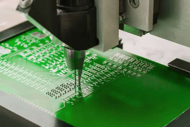
Now, the files are forwarded to a PCB manufacturer, and the next step is to get a prototype board, which will help them know if the design is correct. With the use of 3D printing, designers and engineers can easily detect and address any development flaw that occurred.
Testing and Iteration

The printed circuit boardboard is authenticated to assure that it functions exactly as envisaged. The built prototype will be the follow-up; an arising problem will lead to the design modification which will, then, be decided to make a new one.
Final Production
PCB design files are placed into mass production for further assembly process only after the design is approved and tested. It indeed marks the final stage of our production process. In order to manufacture the endurance product all ready to make printed circuit boards (PCBs), they are then connected with components.
What are the types of PCBs?
PCBs are available in multiple types, with each type, possessing some form of functional purpose and a unique set of peculiarities accordingly. PCBs are classified into many varieties, with each of them having its unique features, and the selection of the one that suits the electronic device it will be used in depends on the function it has to adopt in that particular device. This is a list of some popular types:
Single-sided PCBs
There are integrated components which have one-side tracks boards for copper traces. They are quite cheap and can be defined as “islands of intelligence” which serve well low-density applications.
Double-sided PCBs
Copper is on each side of the board with conductive route traces and plated through hole components which convey a connection between components. They show more reliability and smaller size as compared to the single-sided PCBs that are having components placed on only a single side of the PCB.
Multi-layer PCBs
They can be made of three or more layers of conductor – surrounded by insulator. They ensure that the system faces the growing complexity of the circuits and in addition to the maximum component density. Those scarce materials are essential in making high-tech gadgets or some have alternating layers.
Rigid PCBs
They represent the fixed ones which are made out of solid substrate material and because of the non-flexible nature have the tendency to show zero resistance while walking or running. Through their dominance in electronic devices as the most common PCB, they demonstrate their efficiency in the electronic devices of people worldwide.
Flex PCBs
These are basically FPCs with great deal of flexibility such that they can bend or twist without breaking. These materials are employed in places where bending and other similar properties like in medical tools and wearable devices are demanded.
Rigid-Flex PCBs
These are a range of PCBs that are harnessed together in a single board which is made up of both the flexible and rigid PCBs. They accommodate the advantages of the types represented and are used in cases where flexible and rigid features are needed simultaneously in applications of such kind.
High-frequency PCBs
They are optimized and can handle the trouble-free reproduction of high-frequency signals without loss or interference. They are widely used in division of broadband, wireless telecommunications, and RF apparatus.
How to make a printed circuit board?
PCB manufacturing is a multi-step process, every step of which matters because it is aimed at forming a circuit layout which ensures the proper operation and inefficient delivery of the circuit board with different schematics.
First of all, come up with the circuit on a PCB design software or design a circuit, making a schematic symbols that implies how items are connected.
After that, design and layout the PCB. While schematic is essential, schematic capture is the first task in writing the layout design. Regarding the top assembly, populate components and run traces, taking into account the factors like integrity of a signal route and thermal management in the circuit.
Next, build Gerber files that encompass info on layers on a copper plate, solder mask as well as silkscreen either bottom layer or top layer.
Next process will be addition of fabrication prototyping. We submit the Gerber files to a PCB manufacturer or reference designators to bring your prototype board design to life. This means that on some days you engage in product development and some days you make changes in response to your findings.
Finally, when surface mount technology (SMT) is applied, build the files for mass production PCB design. Connect these files to print circuit board manufacturer machine to facilitate mass production.
Along the way, cooperation from electrical engineers, PCB designers, and constructors become necessary because PCB is expected to fulfill the requisite conditions and is functional.
What are the materials used in designing of pcb?
Print circuit board (PCB) is developed with a range of components, each of them contributing to a unique objective. The following are some examples of common materials:The following are some examples of common materials:
- Substrate – Isolation from all sides and mechanical help happen through the component called substrate, which is the base layer of printed circuit board (PCB). Once the laminate is formed, it will be cured in an autoclave with a pultrusion process. The resin used is a fiberglass-reinforced epoxy.
- Copper layer – Copper, together with metallization, are the material that allow you to have conductive traces connecting the different components. In order to achieve the goal, the copper sheets of narrow thickness are covered with the substrate with laminating technology.
- Solder Mask – a coating that is applied on the top of the copper cables to prevent the infiltration of accidental electrical connections and to shield from the effects of surrounding elements all at the same time.
- Silkscreen –Printed text or symbols on the PCB’s surface mount components, which provides part labels among others to support product installation and service of the same.
- Solder Paste – is a generic name for solder alloy coated with flux. This paste is basically used to attach parts of assembled circuit boards on printed circuit board.
- FR-4 – An epoxy-based flame retardant is usually used for the substrate of the PCBs as the combination of durability and low cost are its key advantages.
- Copper Clad Laminate –there is an impregnation of composite material that is contributing to the manufacturing of printed circuit boards (PCBs). Its construction based on a single layer of copper foil that is glued to the substrate.
- Resist – The material applied on the copper lines with the intention of protecting during etching process, the typical mask used in the process of creating a circuit pattern.
What are the pcb layout capabilities?
Software for PCB design is the program with its features and component pins that a designer uses to create and modify the PCB layout. Hereafter are the functions of PCB layout specifications being described. These are some of the most typical capabilities of PCB layout:These are some of the most typical capabilities of PCB layout:
- Component Placement –Working with electronic components by soldering them on the board shape and moving them around whenever necessary this.
- Trace Routing – Established signal integrity while routing wires between components to finish the connections and pay attention to the electromagnetic interference.
- Layer Stack up – The troubleshooting process of PCB design involves many aspects such as how many layer stackup and what material each layer is made of pcb stack up.
- Design Rule Check (DRC) – In order to avoid any changes in the design during the manufacturing and electrical requirements verification process.
- Auto-routing – Manufacturing mechanically from scratch by automating the routing of copper between components in accordance with certain parameters and reducing the manual effort and time.
- Signal Integrity Analysis – Analyzing the design, to make sure it has no signal integrity issues that can be the problem of Reflections, Crosstalk and Impedance mismatches.
- 3D Visualization – Viewing and checking component clearances and fit in the three-dimensional room to make 3D PCB layout.
- Gerber File Generation – These include the eyelids, the eyebrows, the skull tail, and the mandible.
- Library Management – The library system allows the user to manage the component bank as well as the component footprints and the other design elements that the user use in the different instances.
- Simulation –Stimulating the circuit in the simulated environment to ensure its functioning and performance before proceeding to fabrication.
What is the High-Density Interconnect (HDI) PCB Design?
High-Density Interconnect (HDI) PCB design implies an advanced PCB design that optimizes the space for the mounting of component and signal integrity complex designs. HDI PCBs combines microvias which are associated with high yields breakdown in the conductor edges to the plane, hence better performance. This results in fine traces and spacing, enabling more connections in a smaller area. . Having a stacking substrate of HDI PCBS means that they often have multiple layers and so incorporate material in the upper performance levels. This design is not only perfect for e-devices with limited spaces like phones and tablets but also has fewer packed elements hence saving more space.
How to start a new pcb design?
A clean PCB should be the starting point whenever beginning a new PCB design, as there are many critical steps that must be taken to reach the top of the new board. What follows is a broad guide:
- Define Requirements –This includes setting the component density limits, making sure that all the elements are placed the way they should be, as well as how the PCB should function in general.
- Schematic Design rules – Write a circuit schematic diagram by the use of PBC design software. Identify the components, how they work, and what they are connected to.
- Component Selection – Select parts in accordance to the schematic must be stated taking into account key factors such as size, energy consumption, and physical availability.
- PCB Layout Design – Upload the schematic into a PCB layout software. Placed the components and divide traces into parts and keep signal integrity and thermal management in mind. From >> A Guide to PCB Manufacturing Processes
- Layer stack up –Set the PCB layers detail including the number of layers and the material of a layer which is required.
- Design Rule Check (DRC) – Conduct a design rule check for layout to verify the fab and other needs.
- Gerber File Generation – It will be better for the Gerber files to include all information required for PCB fabrication, which includes copper layers, solder mask and silkscreen.
- Prototype Fabrication – Send to a PCB manufacture and have it produce a prototype board according to the files (Gerber). Trial run the model to ensure it properly operates.
- Testing and Iteration – Even when problems arise, make the necessary modifications and prepare a new design to fabricate another prototype. Reiterate the procedure consistently, until all conditions are met.
- Finalize Design rules – When the artwork is finiset and tested, make the PCB files for mass production ready.
- Mass Production – It is an idea that you might try sending your printed circuit board (PCB) design files to a PCB manufacturer so that you can ultimately industrially manufacture them on a larger scale. Disjoining the board outline from the printed circuit boards (PCBs), they are boarded by the components to finally get the final electronic product.
How long does it takes to learn pcb design?
The period for learning printed circuit board design can be quite a variation based on initial development, design complexity and time investment for developing notions. For the newbies the period will be running from several weeks to several months to get the basics to lower level such as schematics, component placement, and trace routing. There is a chance to become proficient, that after several months to a year and a half of consolidating the knowledge and learning process, you may have been already experienced or in the drill holes. Conversely, the way designers learn continuously and develop with time greater than the period being experienced.
Which software tool is used for pcb design software?
Today most of PCBs are designed with the help of a number of software pcb tools that are different in their features and capabilities and every software has its own specific functions. Included among the most well-known are the following:Included among the most well-known are the following:
- Altium Designer – The industry plugs Altium Designer primarily for the purpose of PCB designing because of its ergonomic and versatile user-interface.
- Cadence Allegro – Expert views saw Cadence Allegro to be an optimal option for it, as it features more permissiveness for high speed and multilayer PCB (Printed Circuit Board) designs.
- Mentor Graphics PADS – the tool that is very often used for the design of the printed circuit boards (PCBs) of small to medium size because it is easy to learn and use. Mentor Graphics Pads is a one of such app.
- KiCad – this software is open-source and it ranges from beginners to small businesses who utilise its cost-effective nature and its community background.
- Eagle – Eagle is indeed a calendar option of choice for hobbyists and small scale businesses. Its user-friendly interface is available you may want to know, and also it is being provided with a set of useful functions.


