The importance of the thickness and understanding the effects of copper thickness in the majority of PCBs at their best is fundamental to guaranteeing the quality and performance of your electronic boards. In this manual, the knowledge of the required copper standard thickness on PCBs and their necessity in electronic board design rules and manufacturing are discussed.
What is a Copper PCB?
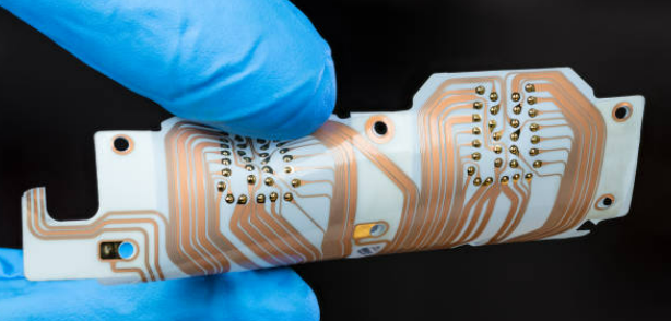
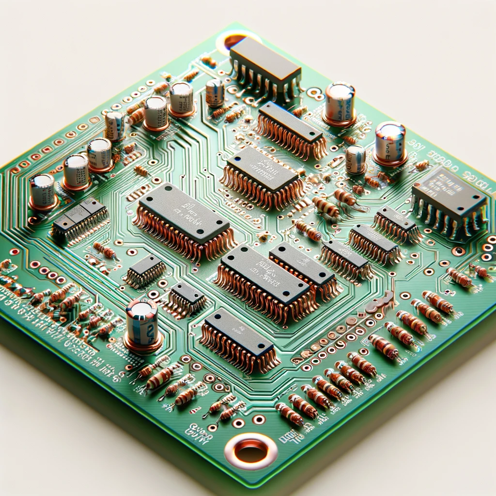
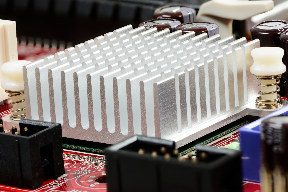
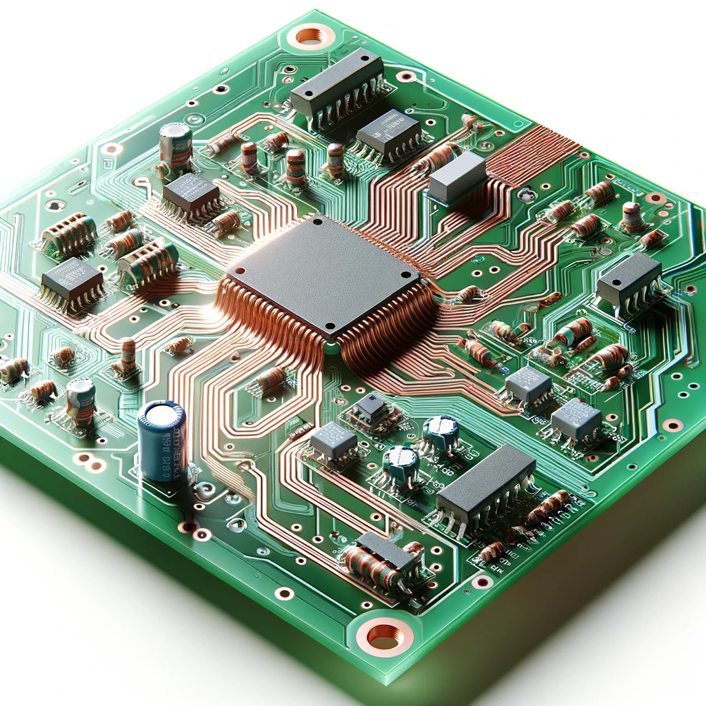
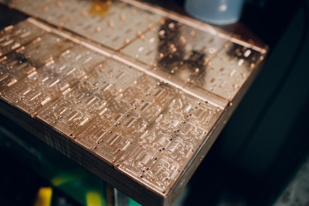
The copper PCB stands for the copper printed circuit board that is a building block of electronic devices and crucially utilizes copper as a conductor metal for its inner layer or internal layers of the wiring network with 1 oz of copper on each layer. The boards usually include an insulating material (like FR-4) with a thin layer of copper either bonded to it or laminated onto it. The PCB thickness of the copper layer can range, with one common measure being ounces per square foot. As a part of the process of etching, the surface area of copper that is desired is removed, forming the circuit pattern. Copper weight in PCBs, high in conductivity, low resistance and low cost provide excellent signal and heat dissipation. Increasedly popular in various fields like consumer electronics, automotive, telecommunications and others, the copper PCB forms the backbone copper features carrying the internal and external layers of its circuits and places of connections, aswell as its copper tracks.
What are the advantages and disadvantages of using a heavier copper PCB?
Using a large number of inner layers of PCB copper and different thicknesses and layers of finished cuprum (Cu) in PCBs offers several advantages and disadvantages, which should be considered based on the standard PCB layer copper thickness of the application:
Advantages of Thicker Copper:
- Higher Current Capacity: The higher cuprum (Cu) replication thickness of a copper trace can be lit without significant voltage drop or excessive heating for the currents. This proves to be critical in power electronics and high-current applications where a large amount of current circulates on the printed circuit board tracer.
- Better Thermal Conductivity: Thicker PCB copper in high technology has more possibility for better heat dissipation from components mounted on the printed circuit board. This facilitates managing the temperature of such components and improving the overall system’s dependability.
- Improved Mechanical Strength: Copper with a thick PCB can serve as a better mechanical support and has the capacity to endure high mechanical stresses while in production or assembly. As a consequence, the reliability and durability of PCBs are high.
- Reduced Impedance: Greater copper thickness traces feature lower impedance, which is beneficial in high-frequency circuits, signal integrity, and transmission line use cases. Low impedance strives to prevent signal loss and distortion.
Disadvantages of Thicker Copper:
- Increased Cost: A higher gauge of copper needs more material, though, for the same result in PCB thickness, which in turn raises the cost of PCB fabrication. Moreover, there might be a need to alter process manufacturing volume in order to produce thicker cuprum (Cu), which leads to higher fabrication costs.
- Reduced Trace Density: It requires more space for board surface copper thicknesses with PCB standard volumes than a thinner copper device. This confines the routing space, which in turn foils the density of traces and complicates the routing of complex PCB layout plans.
- Limited Flexibility: Using a thick copper PCB foil makes the PCB less flexible, which can matter in applications where flexibility is key, such as with FPCB or RFP. Achieving this goal will also be influenced by the PCB’s excessive rigidity and capability to follow the curvature of non-flat surfaces.
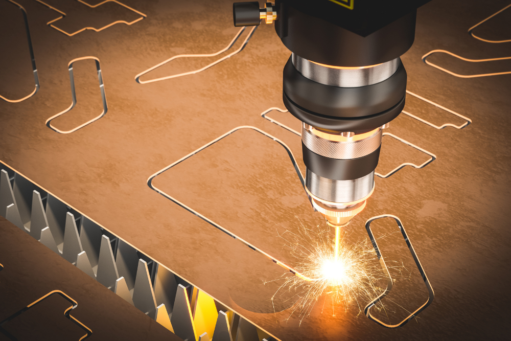
- Increased Etching Time: The copper removal process due to etching of the PCB substrate could take longer as higher-gauge copper is used in the production of PCBs. It can therefore result in longer batch lead times and higher chances for a higher manufacturing cost.
Does the weight of a copper PCB matter?
It is true that the copper weight in a fully soldered copper PCB does count, and copper weight can in fact have major effects concerning the performance, price, and fabrication of the final copper PCB. The copper weight, or technically, oz copper, is usually measured in ounces per square foot (oz/sq.ft) and refers to the total copper thickness brazed or laminated to the underlying substrate of the PCB. Here’s why copper weight matters:
1. Electrical Performance: The width of copper traces governs the board’s electric conductivity and resistance. Thicker copper PCB tracks have the ability to draw more current with less resistance, thus reducing voltage drop and sending more reliable signals throughout the circuit.
2. Heat Dissipation: Copper is an amazing conductor of heat. This class of PCBs can dissipate heat faster, which is an important feature for electronic products that generate heat as they function. Correct heat dissipation techniques will avoid components getting too hot, which will ensure the durability and stability of the PCB.
3. Current Carrying Capacity: High copper gauge wires feature a greater carrying current, which can be employed in applications requiring the running of high-powered systems or big currents. This is particularly critical in power electronics and high-current circuits, respectively.
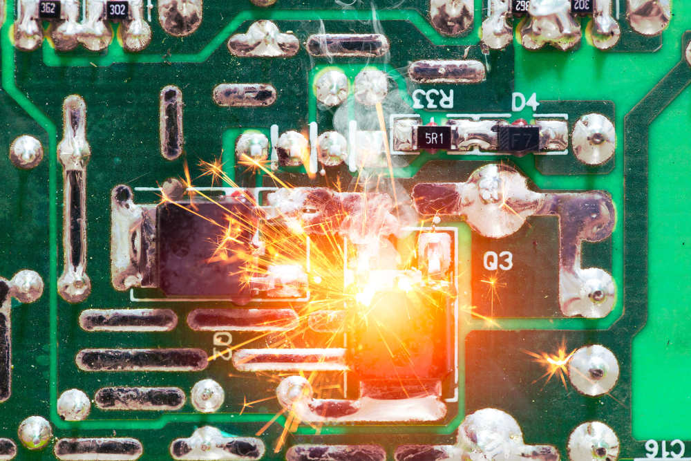
4. Manufacturability: Thicker cuprum (Cu) plating at higher gauge levels may necessitate changes in the PCB manufacturing procedure, for example, a longer etching time or specialized apparatus used. This, in turn, can influence the manufacturing costs and the time it takes to manufacture a product. Along with these, the use of a thicker cuprum (Cu) gauge will add some problems in PCB fabrication, like a higher risk of over-etching and reduced resolution of fine traces.
5. Cost: Thicker cuprum (Cu) sheets need more material, and this is reflected in the high cost of the PCBs. Designers need to pay for both sides of the coin because heavy copper PCBs mean better reliability and performance, but it is also more costly to buy this added feature.
Why Would You Use Heavy or Thicker Copper in a PCB?
Large copper is used for the PCBs majority purposes, namely to address the performance and design requirements and to also increase the reliability and other specifications of the circuits. Here are some key reasons why heavy cuprum (Cu) may have more quantity than the common unit of copper weight being used in a PCB:
- High Current Handling: Copper PCBs with a high current level are capable of supplying electric current without suffering from capacity overheating or being loaded with voltage breakdowns. This is why IGBTs come in handy when sizeable currents that are associated with motor drives, power converters or high-power LED lighting systems are involved.
- Improved Thermal Management: The thick cuprum (Cu) films are more conductive, which enables them to melt heat away faster. It is suitable, particularly in cases of overheat generation by the device, and thus keeps the temperature rise to normal, resulting in an increase in component life.
- Enhanced Mechanical Strength: Copper-printed circuit boards (PCBs) with thicker copper layers provide higher mechanical robustness and add to overall durability. Hence, they are good for use in such applications as a car electronic system, aviation systems, and industrial equipment which is subjected to mechanical stress, vibration, or harsh environmental conditions.
- Reduced Impedance: Additional weight of copper lines are less impedance, which will benefit high-frequency modes and in applications sensitive to signal integrity. A lower impedance helps decrease signal lossdistortion and EMI (Electromagnetic Interference) to ensure efficient data transmission and a system with good performance.
- Increased Reliability: In general, the higher the gauge of the copper PCB, the better its reliability and durability, which are associated with a number of positive features such as higher carrying capacity, improved thermal management and better mechanical strength. They are convenient for applications with high-level mission criticality, where the system fault or failure is risky.
- Design Flexibility: Copper’s elevated weight promotes the revelation of intricate PCB layout with thicker tracks and higher current-conveying capacity. The multifunctionality gives room for tailoring such PCBs to meet specified application needs and improve copper features in PCB quality.
What copper-clad laminate (CCL) thickness is usually used for printed circuit board?
The thickness of the copper-clad laminate in PCBs can be different depending on what thickness is required, the thickness of different kinds of printed circuit boards and the PCB manufacturing process (multiple stack-ups). For example, several thicknesses are commonly used in the industry, in spite of the fact that some common ones are.
Mainly, for most typical PCB usage, copper foil laminates of different copper thicknesses, from 0.5 oz copper thickness to 3 oz total thickness, are a good choice. Here’s a breakdown of typical used copper foil thicknesses and their equivalents in micrometers (microns):
- 1/2 oz (0.5 oz) copper: It is approximately 17.5 μm or microns.
- 1 oz. copper: approximately 35 microns (µm).
- 2 oz. copper : About 70 µm of it all then.
- 3 oz. copper: About 105 µm or microns.
In contrast with the various other selections, 1 oz. copper thickness is often used for standard PCB copper thickness. It is an optimally balanced term between price, conductivity, and simplicity of fabrication. Depending on the type, thickness or cuprum (Cu) (for example, pcb copper thickness 0.5 oz copper or 2 oz copper) may be chosen for simple circuit or applications where cost and weight of components matters. 2 oz. or 3 oz. of copper is required by high-current purpose, power electronics, heat dissipation or electrical designs.
Moreover, the desired thickness of the finished copper weights mostly depends on the power of the circuit board, thermal issues, rigidity and affordability. Design engineers apply the copper thickness calculated per the above factors and the specific requirements of PCB copper thickness.
Conclusion
In summary, copper circuit boards are the backbone of modern electronics, and their unique conductivity and adaptability are what enable them to seamlessly fit into the circuitry of any device and carry out complex signals properly. According to the targeted use of the copper thickness cu weight minimum, the PCBs guarantee reliable electrical performance, brutal heat deflection, and robust mechanical support. Nevertheless, the selection of the copper thickness and finished copper weights is determined after careful assessment, where electrical demand, heat management, manufacture capability, and economic features are all involved in the decision. At times, as the technology continues to advance, the standard and required copper thickness and standard copper weight used in the PCBs change with the aim of facilitating innovations that traverse the spectrum of industries, followed by the unhampered operation of electronic systems globally.


