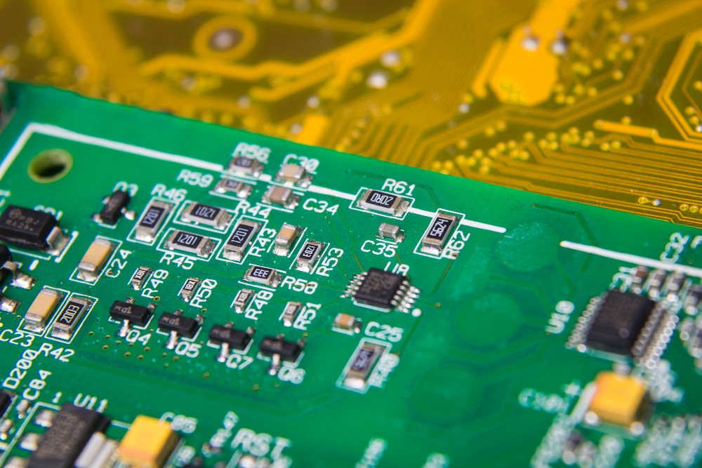
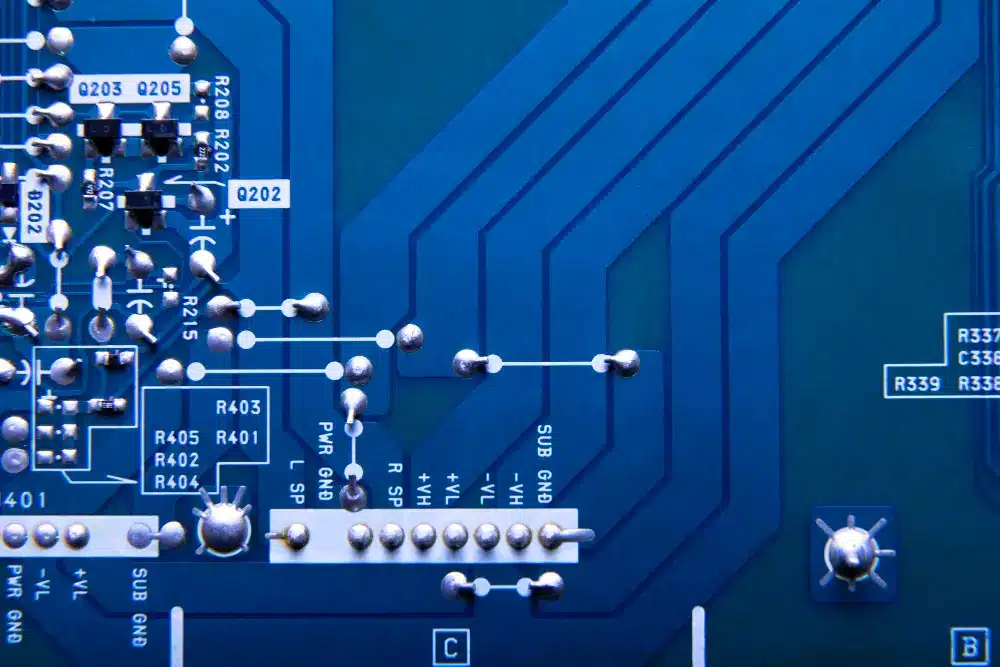
Mastering the Art of Silk Screening PCB: A Comprehensive Guide
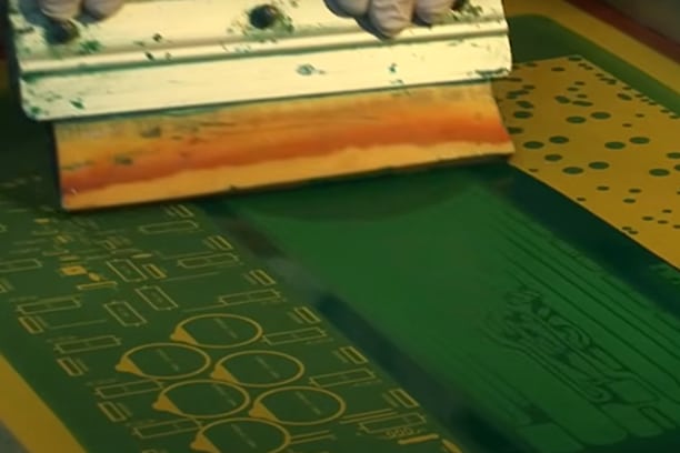
The document titled “Mastering the Art of Silk Screening PCB: A Comprehensive Guide” provides an in-depth exploration of the silk screening process used in printed circuit board (PCB) manufacturing. Silk screening, integral to PCB production, is used to apply text, graphics, and identifiers like component designators and test points directly onto PCBs. This guide covers the steps involved in the silk screening process, which includes design preparation, stencil creation, ink application, curing the ink, liquid photo imaging and final inspections. The technique ensures that components are correctly placed and oriented, which facilitates assembly and troubleshooting. Additionally, the guide discusses the importance of various factors in silk screening, such as ink quality, stencil accuracy, and process control, emphasizing how these elements contribute to the functionality and reliability of the final PCB product. Silk screening not only enhances the assembly process but also serves as a critical quality control tool by incorporating identifiers and regulatory markings directly on the PCB.
Mastering Thru-Hole Technology: A Deep Dive into Durable Connections for Your PCB Projects
THT (Thru-Hole Technology) is a traditional part of PCB assembly, which has been a traditional form technology for quite some time, providing its superior mechanical strength and reliable electrical connections, especially in places that faced such high physical stress and required high power handling to work, such as in the military, aerospace, and automotive sectors or automated insertion mount machines. In spite of SMT (surface-mount technology) and surface mounted components, which are compact, cost-effective, and still flexible for manual soldering, THT (through-hole technology)and through hole component remains superior in that it is still very reliable and easier to handle, making it best for high-reliability applications and environments where sturdiness is the issue that matters most. Such a comprehensive investigation of THT, in turn, highlights the evergreen importance of the THT technology of modern electronics, which implies that THT is used to ensure the performance and good health of electronic components during intense use.
The Ultimate Guide to Turnkey PCB Assembly: Everything You Need to Know
The article titled “The Ultimate Guide to Turnkey PCB Assembly: Everything You Need to Know” provides an extensive overview of turnkey PCB assembly, a service where manufacturers manage every aspect of PCB production from sourcing components to final assembly. The guide explains different types of turnkey services, including full, partial, prototype, and production turnkey PCB assembly, highlighting their specific features and benefits. Full turnkey services are particularly emphasized for providing a comprehensive, one-stop-shop solution that simplifies the entire process for the client. The guide also details the capabilities of turnkey PCB assembly such as design support, component sourcing, PCB fabrication, and testing. Benefits such as cost efficiency, time savings, and quality assurance are discussed, along with the advantages of using full turnkey services compared to other methods. The article concludes by advocating the turnkey approach as a convenient, efficient, and quality-assured method for PCB manufacturing, suitable for businesses looking to minimize supply chain risks and enhance market competitiveness.
Mastering Soldering Joints: A Comprehensive Guide for Perfect Connections
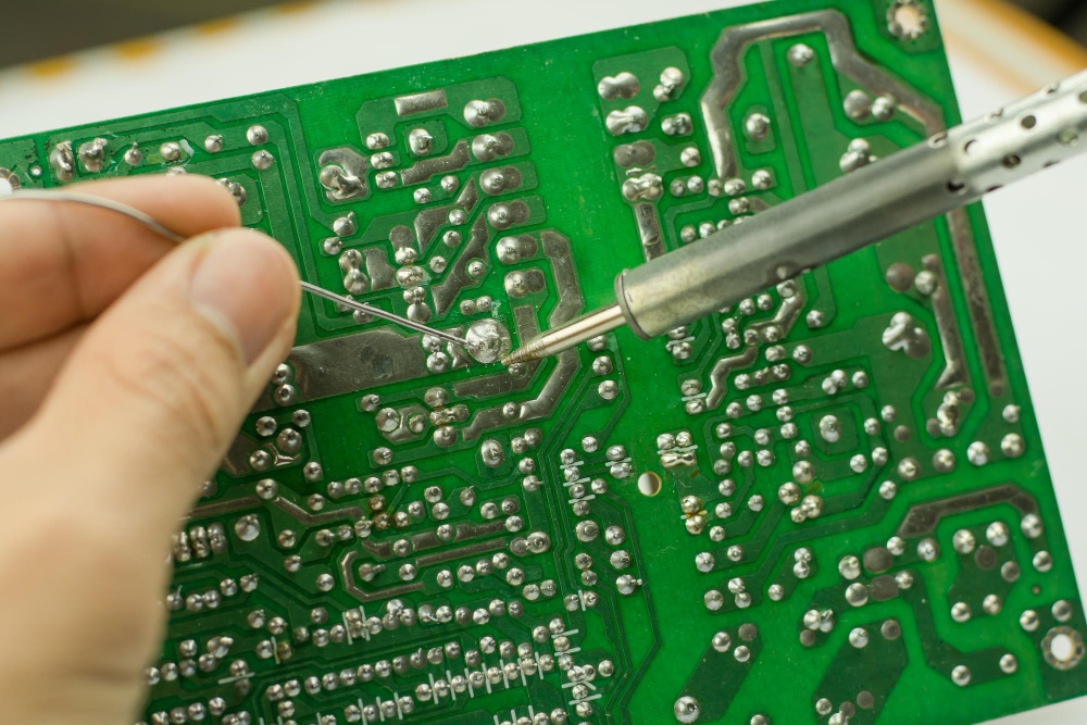
The document titled “Mastering Soldering Joints: The comprehensive guide in “Project Solder Techniques: For Perfect Sales Connections” covers diverse soldering methods that would be helpful in creating strong and robust connections in electronics. It depicts the different soldering joints i.e. Lap, Butt, T-Joint, Corner and Filleted Lap, highlighting the particular fields in which their usage and utility are best. The guide stresses out the fact that to highlight the involvement of relevant instruments and materials, a soldering iron, solder, flux, and safety equipment is essential for a good result. These steps are covered on key soldering topics such as surface prep, joint heating, solder application, and post-soldering cleaning. In addition, guide describing the different types of solder joint problems, such as cold joints and bridges is also provided. Moreover, the guide also suggests ways of keeping those problems at bay. So, the document can serve as a teaching tool for people of different skills level: those who just want to have some experience in the sphere and advanced users who know soldering well and want to be aware of the different types of soldering joints suitable for different applications.
The Ultimate Guide to Via in Pad Technology
The document titled “The Ultimate Guide to Via in Pad Technology” provides an in-depth exploration of Via in Pad (VIP) technology, a PCB design technique where vias are directly placed within component pads. This method is particularly beneficial in high-speed circuit designs where signal integrity is crucial. By minimizing the distance signals must travel through connections, VIP technology enhances signal quality and reduces signal distortion. It also allows for more efficient use of PCB space and improves thermal management by linking component pads directly to thermal planes. While VIP offers several advantages, including space savings and improved thermal and signal performance, it also presents challenges such as increased manufacturing complexity and potential for soldering issues. This technology is typically used in applications where performance and space efficiency are critical, such as in compact electronic devices with high-speed requirements.
PCB Layers: A Comprehensive Guide
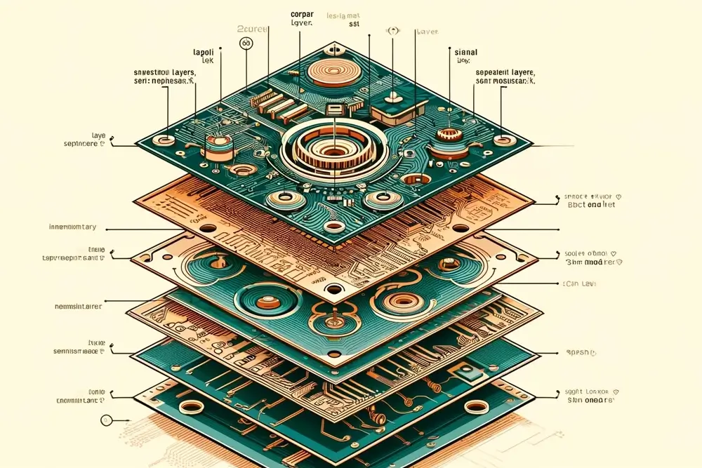
This comprehensive guide provides an in-depth understanding of the different layers of a PCB (printed circuit board) such as the copper layers, signal layers, multiple layers, mechanical layers, outer layers and inner layers and their functions. Explore the importance of each layer and how they contribute to the overall functionality of the PCB. WHAT IS […]
Understanding Standard PCB Thickness Parameters
Printed circuit boards should be designed and produced according to the normal PCB thickness criterion. This is an essential requirement. This paper will focus on the standard PCB thicknesses in electronics and why it matters. What is the Standard PCB Thickness? By the standards in the industry to standard pcb thickness, thickness of a printed […]
Understanding the Role of Surface Mount Technology in PCB Design
SMT Surface Mount Technology is an important way of PCB design. This article discusses the function of SMT in PCB layout and its advantages concerning space, work rate shakeup boosted by swift manufacturing. Understand this technology more deeply, incorporating it in electronic devices. What is surface mount technology? Surface Mount Technology is normally referred to […]
Understanding PCB finishing type: Comprehensive Guide
Various PCB finishing types should be known during building and manufacturing of printed circuit boards. Acquire informed knowledge about different PCB finishes each with its benefits and applications for better performance also the immersion tin finish and lead free finish press. Designing and manufacturing processes of printed circuit boards require awareness of various types of […]
Multi-Layer PCB Fabrication Techniques Unveiled
Learn about the different processes that are involved in manufacturing multilayer PCB to the multilayer PCB manufacturing process either outer layers. In the context of developing multi-layer printed circuit boards, research on advantages disadvantages and applications of advanced types will be required you can also reaf the advantages of multilayer pcbs. The multilayer printed circuit […]