Robotics PCB: Key Components and Integration
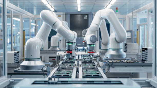
PCBs for robotics are hardware printed circuit boards used in robots and contain sensors, actuators, control units, power supply units, microprocessors/microcontrollers, etc. These PCBs are significant in the operations of robots since they offer the required electrical infrastructure linking sensing, processing and actuating. Printed circuit boards utilized in robotics includes single-sided PCBs, double-sided PCBs, multi-layer PCBs, rigid-flex PCBs, high-frequency PCBs, and high-power PCBs, which are further specialized for function. Outlined below are the various aspects of PCB component robotic manufacturing: Component placement – This is a crucial aspect in the design of a robotic PCB manufacturing system; Robustness – This is a measure of the reliability of the robotic PCB manufacturing process and its subsequent application; Signal integrity – This is also a measure of the reliability of the robotic PCB manufacturing system in its application; Power management – This is also an essential concern for the reliability of the robotic PCB manufacturing
The Ultimate Guide to No-Clean Solder: What You Need to Know
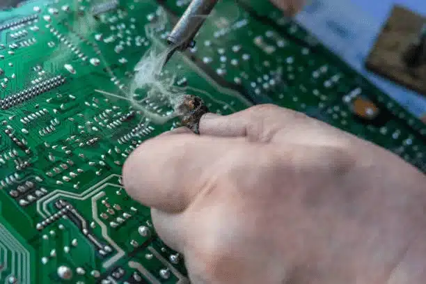
The use of no-clean is a relatively new soldering method that does not require post solder cleaning because it generates a small amount of non-reactive residue. This method makes them be productive, save time and also the cost of manufacturing. No-clean fluxes are made to be non-conductive and non-corrosive to provide solder joints with the durability of no-clean flux without the cleaning processes. Some examples of no-clean flux include rosin, water-soluble, halide-free, low-solid rosin and synthetic materials suited for particular applications. The no clean soldering method is time and cost effective and it is friendly to the environment but it does not work effectively on some components and there are also cases where residues are formed that may impact negatively on some delicate applications. No-clean soldering is therefore a more practical approach of soldering that does not sacrifice reliability and cost-effectiveness.
The Importance of Soldermask in Electronics
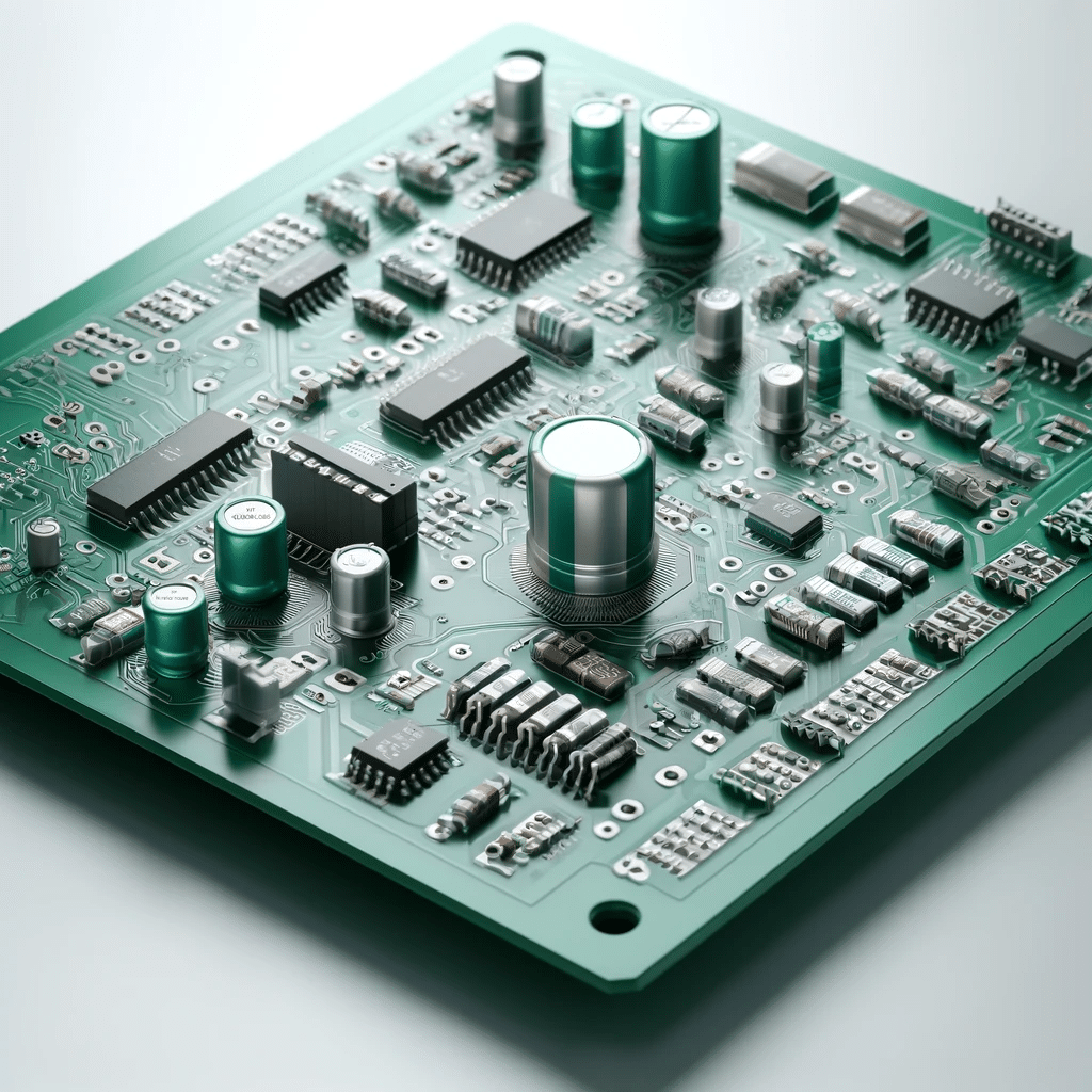
The soldermask is an essential layer for the manufacturing process of PCB since it protects the conductive traces from outside agents while also serving as an insulating layer. It eliminates the possibility of short circuiting, protects against environmental factors, moisture, and chemicals, also makes devices more reliable and long lasting. Soldermasks are also useful in the assembly in as much as it improves solderability besides affording the ground for giving alignment aids for components. They also vary in color so as to create easy identifications and branding. Soldermask can be applied by screen printing, spraying, or photo imaging techniques; afterwards, it is cured to achieve a bond to the board surface. Soldermasks act as protective barriers between the boards and their environment, and therefore, help control defects and enhance easy and effective assembly, in order to produce quality electronic products.
Understanding Burn-in Testing in Electronics industry
Over the years, burn-in testing remains to be a necessary process in electronics manufacturing industry because it is aimed at discovering potential issues or defects of products before they hit the market. Learn in detail about the notion of burn-in testing and how it affects positively to both quality and reliability of products. What is […]
The Ultimate Guide to PCB Functional Test: Everything You Need to Know
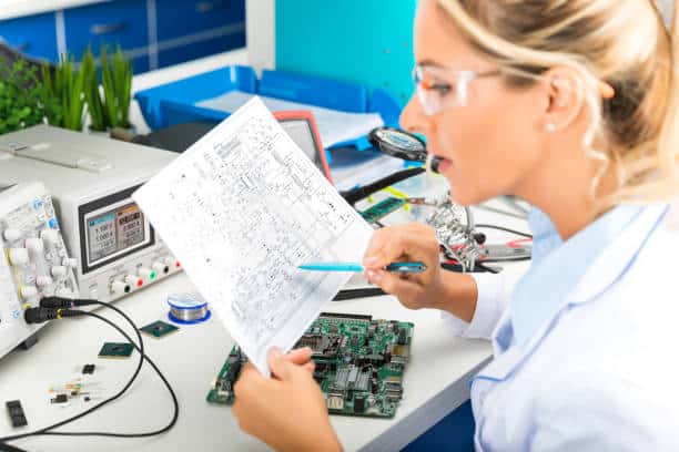
In-circuit testing, of which this is a kind of electronic testing, is usually accompanied by other various techniques. 2. Flying probe testing is a non-destructive method that is employed to find the issues with connections and components. 3. Automatic optical inspection (AOI) is achieved with high performance, high speed and high accuracy visual inspections. 4.Burn-in […]
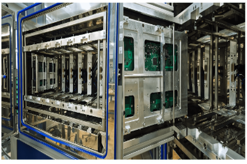
What is the PCB Lamination Process: Everything You Need to Know
The article explains the process of lamination of printed circuit boards. This process is vital for the fabrication of multi-layer PCBs through deposition of layer by layer using heat, pressure and glue to bond them together to make them stronger mechanically and to enable the functionality. It gives the detailed instruction of various lamination processes like sequential, prepreg, vacuum, press and standard lamination, which are chosen depending on what the printed circuit board (PCB) needs. The main reason for the importance of PCB lamination function is its role in maintaining the board’s structural integrity and reliability against a wide range of environmental conditions. To this end, the article provides a detailed instruction on the PCB lamination process as well as information about the material utilized in the PCB lamination. Such components include prepreg, a core material, a copper foil, glue and solder mask. Besides that, the text explores the major issue of delaminating and warping, which happens due to inaccurate control and assurance of quality. To conclude, printed circuit board (PCB) lamination is a crucial aspect in the provision of quality and long-term electronic devices. This is particularly true in cases of electronic parts, where complexity is also increasing.
Understanding PCB Cost Estimator Factors
Understanding the components that make up a cost of PCB (Printed Circuit Board) is critical in electrical planning and budgeting. This tutorial provides information on some main aspects PCB cost estimators consider, as well as the impact those factors have over project costs to the printed circuit boards. What is Printed circuit board? The process […]
Mastering the Art of PCB Quick Turn: A Guide to Rapid Prototyping and Production
As the rapidly changing world of electronics design requires a short turn-around time for getting products from imagination to production line, quick-turn PCB design capability will provide a feasible solution to challenge the competition. This guide covers the threshold topics of prototyping and production very quickly, distinguishing between quick-turn services specialized for diverse projects that range from simple prototypes with basic to advanced technology to more complex flex and rigid-flex, prototyping, assembly, and turnkey solutions. The role of these services in this regard is not only to speed up product development but, in addition, to ensure that quality is maintained with shorter lead times. The ability of PCB Quick Turn for builders to cut greatly down on time-to-market is a plus, which, among other things, facilitates faster innovations and speedy reactions by way of market demands in quick turn pcb services.
Surface Mount vs. Through-Hole Technology: Choosing the Right Electronic Assembly Method
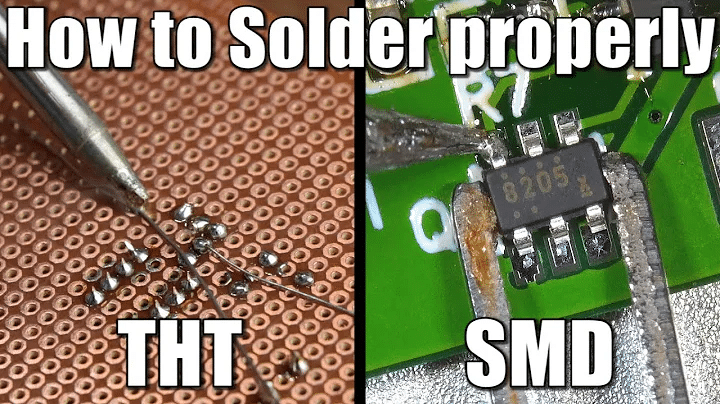
After SMD (surface mounted device) and THT (through hole technology), there is a study called “Surface Mount vs. Through-Hole Technology: It is “Choosing the Right Electronic Assembly Method.” There are examples of the methods and systems used in the field, as well as the pros and cons of each technology.
It’s clear that SMT is great because it handles the space issues that come up when putting a lot of components on a PCB, which makes sense given the needs of today’s small electronics. This technology is known for being cost-effective in large quantities, having better electrical performance from shorter shot trace lengths, and being able to be used in automatic assembly processes.
When strong electrical links are needed along with good mechanical bonding and performance under mechanical stress, THT is the way to go. This makes it useful for making prototypes, fixing things, starting over, and working in places that support stability. The built-in sensor lets you change parts and make adjustments by hand, which is good for safety and educational purposes.
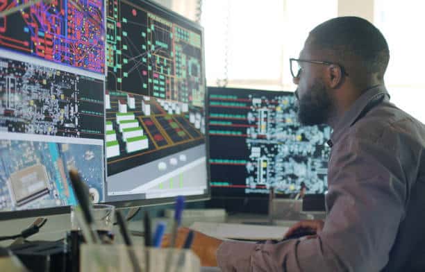
Mastering PCB Design Guidelines
Take considerable time to learn the fundamental PCB design rules and regulations in order to get the hang of printing circuit boards (PCBs) through artful designing. Proper and perfect PCB designing is key. In this article, we explore these tips. What is a printed circuit board (PCB) Layout? The design process of Printed Circuit Board […]