Mastering PCB Design: Your Essential Guide to PCB Trace Width—Latest Updates and Techniques
The document titled “Mastering PCB Design: This essay, which bores down on the relevance of trace width in printed circuit board (PCB) design, seeks to offer an extensive view of its concepts and execution methods. It indicates that trace width control is a vector for current capacity management, signal quality, module robustness, and heat removal in PVCs. With the guide tackling the newest developments in materials and technologies impacting trace width, e.g. high-transition-temperature (Tg) FR4 and polyimide for high temperature applications, as well as HDI technology to build a more compact and efficient PCB layout. Besides, thermal management methodologies such as managing temperature levels on print circuit boards with traces with small widths are also included in the discourse. The publication gives readily applicable information related to calculations of ideal trace width, while taking into account the influenced factors that include the current load, temperature increase, and copper thickness, by PCB trace width calculators. Thus, it can be viewed as a complete manual for PCB designers who want to take their products to the next level by selecting the appropriate trace widths to get better performance and reliability.
Trace Width vs. Current: Essential Knowledge for Optimizing PCB Performance
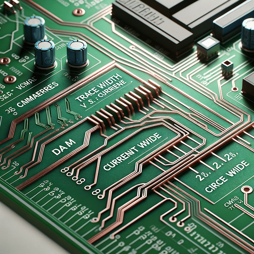
The document titled “Trace Width vs. Current: The article “The Binding between the Two: Dig into the Trace Width and Current Carrying Capacity in Printed Circuit Boards (PCBs) Design” is a detailed discussion on the vital aspect of link between trace width and current carrying capacity in PCB designing. It explains the fact that bandwidth of the conductive paths on a PCB can be either too wide, therefore causing the traces to overheat and eventually melt, or be too thin, resulting in some of the current not being delivered and thus damaging the board itself. The guide considers such factors as temperature rise, thickness of circuit traces, trace length, surrounding high temperatures, and thermal pathways. Moreover it illustrates tracing width calculators, deriving formulas and giving a full description to determined the most optimal trace width concerning the current load and temperature limitations. This resource including trace width calculation, accurate sizing for both thermal and electrical issues, is just invaluable for printed circuit board designers who target minimizing the risk of the electrical issues related to excessive heat.
Understanding Cold joints solder: Causes, Consequences, and Solutions
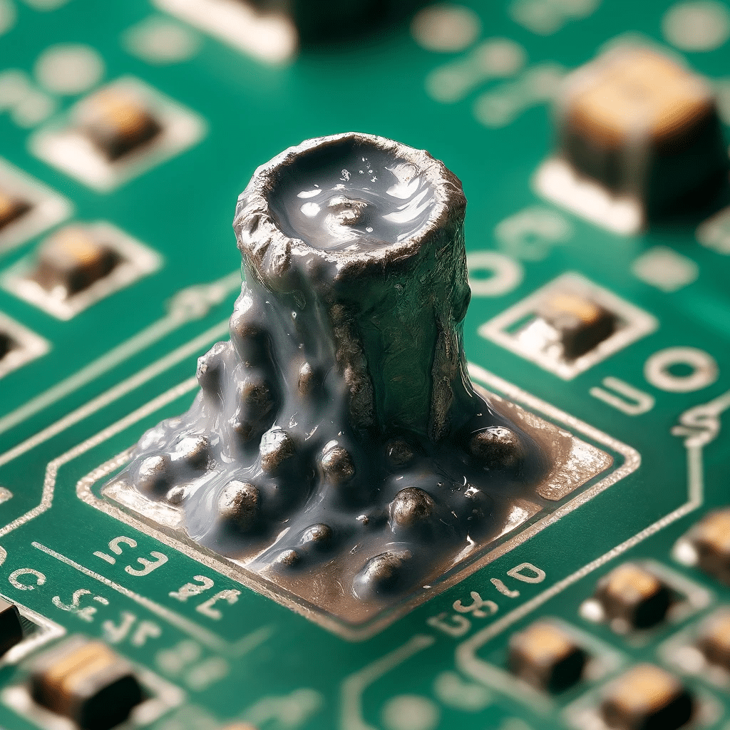
The document titled “Understanding Cold Solder Joints: This work, “Causes, Consequences, and Solutions”, gives an insight into the factors related to the cold solder joints that are troublesome to the electronic manufacturing industry, which then explains the root causes, their effects, and potential solutions that are available. Such joints are caused by the solder that is unable to properly melt down during the first soldering tip operation which results in not-so-good joints which may fail under mechanical stress or thermal fluctuations. This visual symptoms contaminate children’s plastic toys, connected watches, mobile phones, and other flexible permitting the defect with increased electrical resistance, intermittent contacts, and eventually to average electronic device failures. The guide shows techniques to stop these problems from solar joints from getting small, i.e. the right heating of the solder, that required optimum amount of flux, the right type of solder, and utilizing the proper soldering tips. Besides, it presents also the correct practices to find and recover these errors in order to give a quality and durable electronic components. This all-round summary is vital for the people who work in the electrons industry to acknowledge and to fix the smartest unique issue, which is selling, for the purpose of improving the quality of PCB assembly.
Mastering the Art of Soldering PCB: Techniques, Tips, and Best Practices
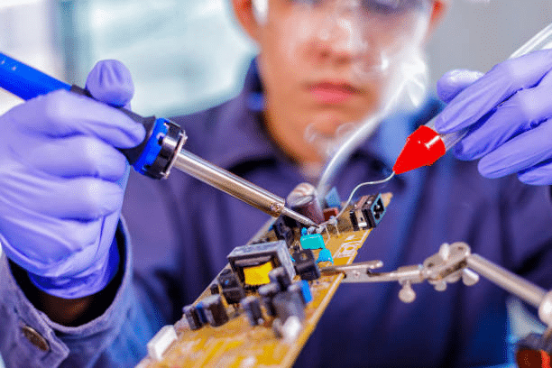
The document titled “Mastering the Art of Soldering PCB: “Techniques, Tips and Best Practices for Assembly of Printed Circuit Boards using Soldering” is the ultimate guide for soldering experts involved in the manufacturing process. It deals with all sorts of soldering technologies appropriate for the usage in various pcbs including reflow soldering, wave soldering, selective soldering, hand soldering, laser soldering and induction soldering, which are designed for specific type of printed circuit boards features and component necessities. The guide includes instruction about the suitable techniques and equipment, which are soldering irons, flux, and lead free solder, that are coupled with the modern development specifically in the low temperature soldering and innovative flux formulations to reinforces an effective soldering and prevent voiding and bridging. Additionally, it must address faults in common PCB solders like cold joints and solder bridges, and instruct the right approaches to obtain the highest quality spring solders. The intent of this cascading manual is to give basic knowledge as well as expertise for both beginners and experienced people to make safe, strong, and consistent soldering connections.
Decoding PCB Tg: Understanding Glass Transition Temperature and Its Impact on Circuit Board Performance
The document “Decoding PCB Tg: To get deep knowledge about Glass Transition Temperature (Tg) and Its influence on the performance of printed circuit boards (PCBs) and the detailed paper “Glass Transition Temperature and Its Impact on Circuit Board Performance” have only one purpose. The Tg values for a PCB is an essential parameter that identifies its endurance capability in terms of serving a mechanically stable function while maintaining its design at higher temperatures. The write-up indicates that the Tg of a PCB substrate represents the transition temperatures (from rigid to softer), which impacts thermal and mechanical properties. This is especially true in circumstances with elevated PCB temperatures, where the particle properties (such as peeling and bending) can be affected if the Tg value goes down. High-Tg PCB are a must in the power-intensive electronics domain, such as automotive, aircraft, and industrial applications where reliability under thermal stress is necessary. An other from the article is that the manufacture is run the consequences of Tg. Therefore, there is a need for materials with a higher Tg than the temperatures the soldering might encounter in order to avert production issues.
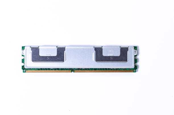
Decoding Copper Thickness on PCBs: Essential Insights for Optimal Performance
Conformal copper in PCBs is a vital factor that maintains quality and performance. Copper PCBs find application in a wide range of different industries starting from consumer electronics and ending up with automobile sector where different copper layers are measured in the ounces per square foot. Higher copper layers offer bigger current density, higher thermal conductivity, enhanced strength, reduced resistance and cost but also restrict flexibility, decrease trace count, elongate etching time and cost more. Selecting the copper thickness which normally ranges from 0. It ranges from 5 to 3 ounces per square foot, strikes a fine equilibrium between performance, manufacturability, and cost, thus providing both electrical reliability and sufficient mechanical support.
The Ultimate Guide of Mastering PCB Design Guidelines
This article looks into the most crucial aspects of PCB (Printed Circuit Board) design. Thus, following the fundamental rules of design for high reliability in electronic gadgets. It get’s to the point that the placement of components part, trace routing, signal integrity, power distribution, thermal management, and manufacturability are addressed. Design software’s also demonstrated the applied techniques and their effect on industry standards towards PCB design principles. These fundamental design techniques that distinguish between correctly designed PCBs and defective ones are the main focus of this stand-alone handbook.
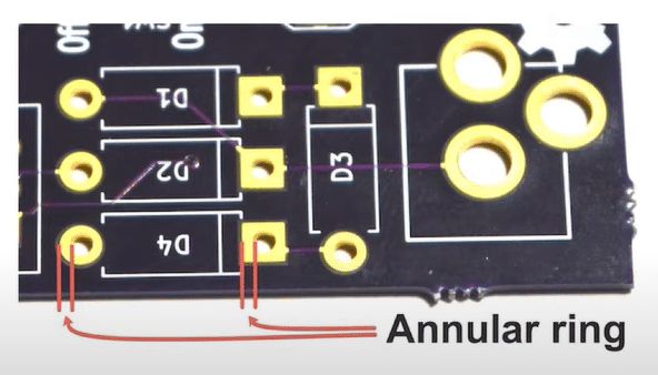
Annular Ring PCB: Benefits and Applications Unveiled
Fast and timeliness fabrication of printed circuit boards enable the quick changing and hence reduces the time taken to bring a new product to market. This method is affordable, helps the identification of a design issue at a preliminary stage, and increases interaction amongst the crew members. Main goals: procedures should be defined clearly, appropriate materials and equipment should be employed, reliable manufacturing companies should be used, and each development stage should be checked and recorded
The Ultimate Guide to Rapid PCB Prototyping: Key Benefits & Best Practices
Rapid PCB prototyping provides the following advantages: faster time-to-market, the ability to manufacture inexpensive iterations of a design, and identifying potential issues with the layout at an early stage. Such a system enables designers to easily draw out and develop prototype boards in as little time as possible in what ultimately translates to shorter development cycles and improved quality of the final product. Through the possibility to go through different rounds at a cheap price, the ability can easily improve on the existing designs hence improving on the ability of cross team members to come up with better solutions. In order to fully harness the benefits of highly-accessible PCB prototypes, there some key areas that should be given specific attention: proper objectives setting and choice of materials and tools, cooperation with reliable manufacturers, along with strong testing and documentation of each prototype iteration.
The Ultimate guide of Cold Joint Solder: Causes and Solutions
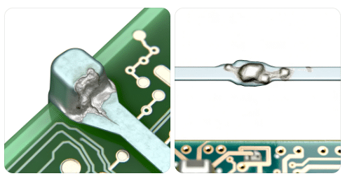
Cold solder joint is the sold ring defect in electronic industry which presents dull grainy appearance and lack of mechanical strength of soldered links and liable to cause circuit failure. Reasons may include insufficient preheating, poor melting of the flux, dirty workpiece or surfaces, improper techniques, quenching, part shift, material defects, etc. Identification methods include appear – and – feel inspection, magnification devices, electrical testing, and thermal imaging. In order to repair, desolder and clean a joint, one must apply flux and resolder accurately. Some of the most common practices for prevention include: The right heating, flux application and surface preparation Correct techniques during brazing Avoiding rapid brazing joint cooling During brazing you should ensure that your brazing joints are thoroughly inspected. Durable connections helps in the strengthening or the improving of the functionality of the electronic devices.