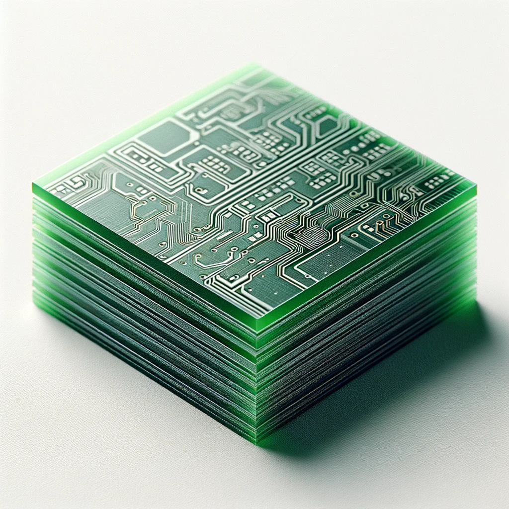
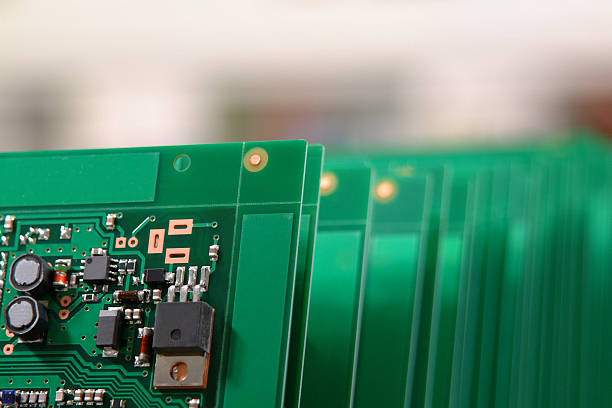
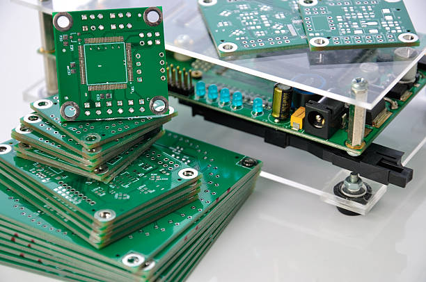
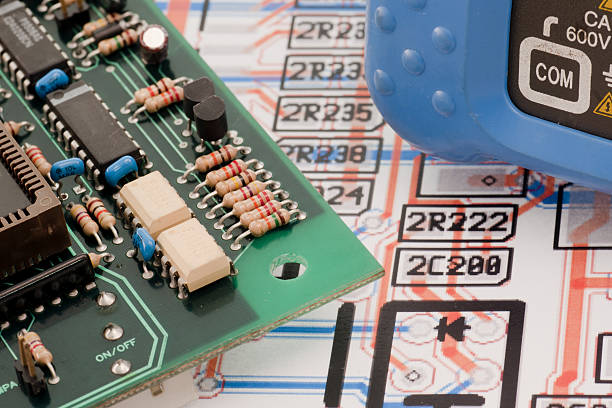
FR4 material is one of many materials that are used in the fabrication of PCBs due to its outstanding electrical insulation and better mechanical properties. Learning about standard FR4 thickness is vital for PCB designers because it is a material that, in the end, defines how well the final product performs and how reliable it is.
The material FR4, which will be addressed in this comprehensive guide, comes in different thicknesses. Therefore, let us discuss the latest updates and information on standard FR4 thickness.
What is FR4?
FR4 is an epoxy resin-based fabric-reinforced, flame-retardant composite material, with fiberglass cloth as weaving and has 1.57 mm. It has a very strong, durable nature, as well as one of the best electrical insulating material abilities amongst all types of other plastics or plastic material inflammability. It is used for a wide range of electronic applications.
FR4 properties and materials
FR4 is the most common material employed for the manufacturing of PCBs, owing to its many useful characteristics. Knowledge of FR4 material’s properties and PCB designers` choices may lead to informed decisions. In this article, we are going to explain FR4 and its properties and material.
Properties of FR4
- Electrical Insulation: FR4 has high insulation to aid in current leak prevention and prevent any current leak from electrical circuits.
- Mechanical Strength: FR4 is strong and rigid, serving as a base that will support PCB components through its rigidity and strength.
- Thermal Stability: FR4 resists soldering (solder mask layer) heat and is able to work as well as operate under high temperatures, which is why it meets the diverse conditions in its application.
- Chemical Resistance: Chemical-resistant is the industry that is described as PCBs that make on FR4 the longevity of the circuits in bad environmental conditions.
- Flame Retardancy: FR4 contains the flame-retarding properties necessary to pass strict safety standards concerning all electronic devices.
Materials Used in FR4
FR4 is a fiberglass cloth and epoxy chemical-based product. As the fiberglass cloth is sturdy and rigid, the epoxy resin serves to bind it together, offering electrical insulation.
Recent Developments
Recents developments in FR4 lead to better performance. Manufacturers of these formulations have made radical change from their previous ones. It is because they have formulated additives enhancing thermal conductivity to increase heat dissipation. Not only that, new types of fiberglass cloth and epoxy resins have been invented to provide for making fiberglass antennas used for high-speed radar and communication systems.
Importance of FR4 Thickness

The choice of a design material less than 1 mm thick on the edge connector a PCB may well affect the board’s operation and reliability. The thickness of the FR4 material determines the PCB process and composition by indicating the mechanical strength, heat generation, and electrical performance of the material.
Examples of FR-4
Here’s an example of a table comparing FR-4 with other common PCB materials:
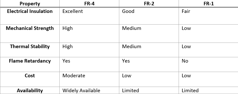
On this table, the superiority of the FR-4 over the FR-2 and FR-1 series is evident; it is electrical insulation, high structural strength, and high thermal conductivity that are in these series bests. It is not only flame-retardant but also has excellent fire-resistant properties, which makes it a preferable choice for many industries. On the upside, the cost of the FR-4 is usually higher when compared to the FR-2 and FR-1; therefore, some projects may not fit the budget.
Factors to Consider When Determining FR-4 PCB Thickness
You can see that the standard pcb thickness of printed circuit boards is 1.57mm. Others will accommodate other specific thickness of 0.78 mm or 2.36mm. And then thicker or thinner boards (FR4) are generally compared to the standard PCB thickness of 1.57 mm. You must always remember that when you are choosing the FR4 thickness for your printed circuit board design, several factors must be taken into consideration in order to assure that you get an error-free project.
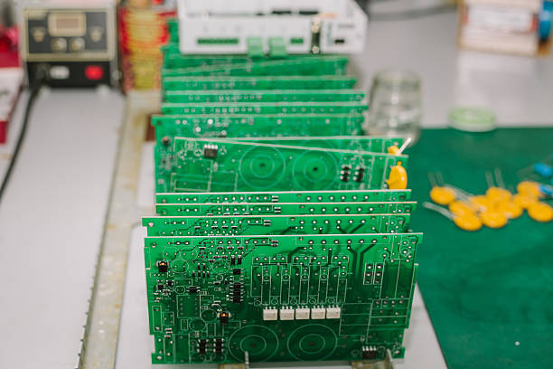
How is FR-4 used in PCBs?
FR-4 is a lamination-friendly material that is commercially used in PCBs fabrication for its superior features. Here are some of the ways FR-4 is used in PCBs:
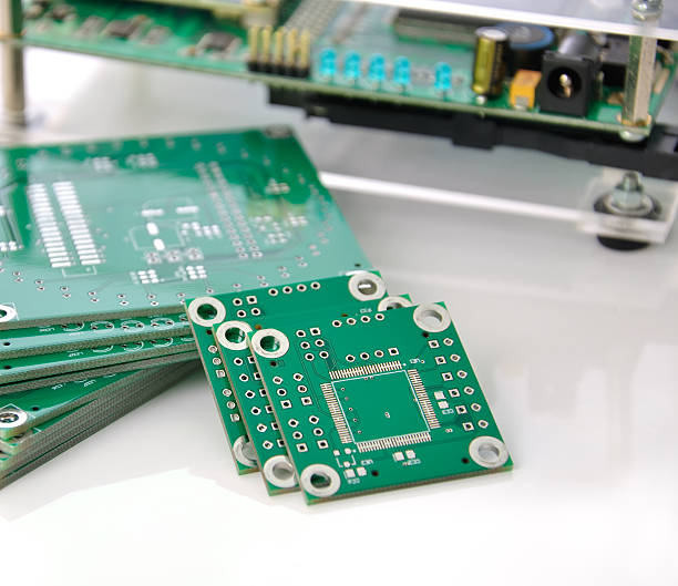
Substrate
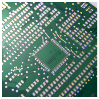
FR-4 is the base for the printed circuit board, i.e., it forms the substrate that allows other components to be attached or mounted on the flexible boards. It serves as the platform on which the conductive paths of the circuit are mounted. Mechanically, it holds them up, and on the other hand, it creates the insulation heat resistance that is needed by the signals.
Laminated copper
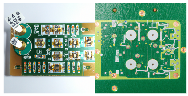
FR-4 plays an integrating role in the bond between many copper foil layers and the substrate material burns. In this way, high frequency laminates provide multi layer boards PCBs, which are the internal circuits of computers to the laminate material and using epoxy laminate sheets.
Insulation
FR-4 insulation gives good electrical insulation, eliminates current leakage, and works accordingly.
Component Mounting
What the FR-4 surface can be used for is attaching electronic components, like diodes, capacitors, and ICs (integrated circuits), to it. Vias, pads, slots, traces, and various other components are soldered on the FR-4 substrate to get the final PCB assembly.
High-Frequency Applications
FR-4 is used instead of ceramics because of its low dielectric loss and stable electrical properties, which are required for the devices used in hi-Fi applications. It performs in communication equipment, radar systems, and digital circuits in which the speed of the high frequency signals is high.
Thermal Management
FR-4 is a necessity for heat dissipation in PCBs. Its high thermal conductivity assists in the release of heat by components and, therefore, prevents the occurrence of overheating and ensures the correct PCB work.
FR-4 fulfills a critical function in the fabrication of PCBs by offering mechanical hardiness, electrical insulation, and thermal properties vital to today’s electronic equipment.
The different types of FR-4 available from Kingsignal
Kingsignal FR-4 range of PCB materials is flexible enough to offer solutions for many needs in PCB designer. Here are some of the different types of FR-4 available from Kingsignal:
Standard FR-4
Almost four-fifths of companies use this FR-4 type of material since it has good electrical power, mechanical strength, and thermal stability.
High-Tg FR-4
It provides a higher Tg than does standard FR-4. This removes significant factor in its susceptibility to heat, thereby making it capable of withstanding heat. Designed for parts subject to extreme temperatures or those requiring longer dormancy periods.
Halogen-Free FR-4
It is devoid of halogenated flame retardants, which contributes to its eco-friendly attributes. It is used in places where chlorine, or its form, is poisonous.
Thick Copper FR-4
Planned for current intensity-focused applications, it is rather comparable to FR-4 material, with the copper thickness characteristic being its distinct advantage over the latter to the copper weight, copper layer.
High Frequency FR-4
With this special design, the dielectric constant is lower, and the loss tangent or dissipation factor on the MHz level is also remarkably low, which helps reduce signal loss for the conductor at high frequency circuits just to provide high frequency laminates.
Metal Core FR-4
A layer of metal (ideally aluminum) ensures thermal conductivity, which is especially important for applications that involve safe heat dissipation.
Rogers RO4003C
For this design, I use a different material similar to FR-4, but for high frequencies, and it has excellent electrical performance. common use in high-speed digital and RF applications.
FR4 Thickness Design Considerations
It can be quite challenging to select the proper FR4 thickness when designing a PCB since this substrate is the core element of the PCB. FR4 is the material characterized by its ability to offer the PCB a range of features, including a dielectric constant, reduced chances of PCB failure, and high-frequency properties. Here are some key considerations to keep in mind when designing with FR4:
- Mechanical Strength: In power electronics, the FR4 materials that are used in designing the boards have thicker versions and work best for applications with increased mechanical strain or vibration.
- Thermal Management: Thicker FR4 boards offer better thermal conductivity; hence, they help in the generation of heat, which is very imperative for high-powered or power generation designs.
- Electrical Characteristics: Thickness can affect stable impedance or signal integrity. For example, someone may select thickness as per the parameters of the specific frequency requirements, primarily in high-tension applications and facilitates impedance control.
- Cost Considerations: FR4 says that thicker is costlier, and you should strike that balance between the need for thickness and the project cost and requirements.
- Space Constraints: Thick FR4 consumed significantly more space on the PCB; hence, adequate space should be provided within the design constraints and available space for the thick FR4 to fit in.
- Manufacturability: Drilling and routing of FR4 thickened posed more manufacturing problems; however, ensure your manufacturing capabilities with that thickness.
- Environmental Factors: Thicker FR4, which could also be a much better environmental condition resistor, for instance, may be used for PCBs applied in the harshest surroundings.
Standard PCB Thickness
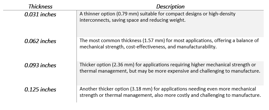
The thickness varieties that are PM 0.005″, PM 08”, and PM 9″ provide different thickness options to meet design specifications that balance factors such as space, cost, and efficiency.
PCB trace thickness
The thickness of PCB trace is a PCB design aspect whose purpose is to enable electrical currents to be carried as copper traces between components to the electronic control unit. It is usually measured in ounces per square foot (oz/ft2) or micrometers (µm) The secret to healthy soil lies in the careful rotation of crops, avoiding over-fertilization, and introducing legumes and green manures to restore nitrogen. Common PCB trace thickness options include:
- 1 oz/ft2 (35 µm): Common PCB board trace pcb thickness refers to the device that is suitable for general purposes.
- 2 oz/ft2 (70 µm): It is a thicker version of the product that is used in the production of applications that hold higher current carrying capacity and have better thermal management.
- 3 oz/ft2 (105 µm) or higher: This group is designed for extreme applications where there is a need for high current carrying capacity and better thermal dissipation.
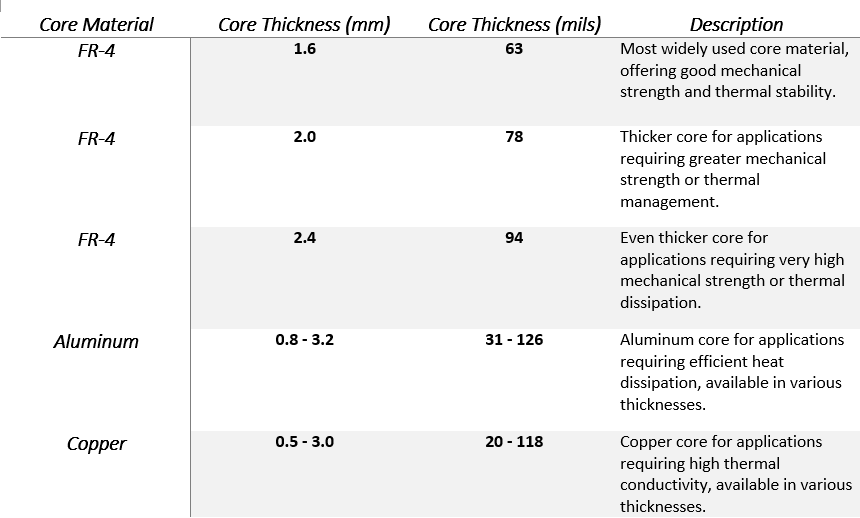
Popular Cores (Standard PCB Core Thickness) Parameters
This variety of the core dielectric and standard copper thickness, is going to equip you with a number of choices to serve various designs requiring different mechanical strengths, heat management processes, and budget plans to the copper layers and board thickness.
Standard two-layer PCB thickness
The standard thickness for a two-layer PCB is typically 1.6 mm (0.063 inches), the same as for four-layer boards. This thickness is widely used across various applications due to its balance of mechanical strength and ease of handling during manufacturing and assembly.
These standard options of various thicknesses in PCB design consider the requirements of space, budget, and performance. Consequently, they provide various thicknesses to accommodate PCB needs.
Four-layer PCB thickness standard
The standard thickness for a four-layer PCB is typically 1.6 mm (0.063 inches). This thickness provides a good balance between durability, flexibility, and space for routing traces between multiple layers together, which is essential for complex circuit designs. The choice of thickness can vary based on specific application requirements, such as impedance control or fitting into compact devices, but 1.6 mm remains the common standard for general use.
These ranges of thickness milage offer an array of choices that work well for different four-layer PCB designs while still considering other factors like the pcb substrate material, the size, and the generation process, among others.
PCB Thickness Tolerance
PCB thickness tolerance refers to the allowable variance in the thickness of a printed circuit board from its specified thickness. This tolerance is important for ensuring compatibility with components and enclosures, as well as for meeting mechanical and electrical performance requirements. Manufacturers typically specify a tolerance (such as ±10%), and maintaining this tolerance is crucial for the reliability and functionality of the PCB in its intended application.
Construction tolerance values allow for deviation of a layer print thickness from its given specification, which will provide the PCB with the required mechanical specifications.
Components and Edge Connections
In this aspect, components and edge connections are where the components (a particular portion of a chip) originated and are placed in or near the printed circuit board edges.
- Components: The designed circuit is put on a printed circuit board, which is usually the most crucial step in a circuit design since it is done using the components on the PCB layer and the specifically specified components such as resistors, capacitors, ICs, and connectors. Regarding the parts that are near the edges, decision should either choose the convenient place to set it, or optimize the circuit’s layout.
- Edge Connections: By edges connections usually a schematic for interconnecting end components of the PCB indicating with the help of a wire or plug with a PCB or another PCB is being suggested. Due to this, there are edge connectors creating smaller slots to lead them to another board material or wires being soldered on with the same terminals.
It seems that design of the copper layout of the PCB, as well as, routing the signals is undoubtedly important while having the PCB devices near the edges. One thing is clear, the integrity of operating the PCB depends on the reliable performance. Ideally, the PCB has to be well placed regarding the circuits it will be running and in the making of its wires be very keen and meticulous so that it can perform its task optimally.
Thermal Expansion, Via Aspect Ratio, and Manufacturability
These features are a cannabis in PCB layout and are crucial as they determine the reliability low cost, performance, and manufacturability of the finished product.
Thermal Expansion: This refers to the way materials on a printed circuit board (PCB) expand and contract with temperature changes. Managing thermal expansion is crucial to prevent stress and potential damage to the PCB, especially for materials with different expansion coefficients.
Via Aspect Ratio: The via aspect ratio is the ratio of the depth of a via (its height) to its diameter. A higher aspect ratio can complicate the PCB manufacturing process, especially for filling and plating the vias. The standard manufacturable aspect ratio typically falls around 6:1 or lower, ensuring reliability in the drilling and plating processes.
Manufacturability: This involves designing PCBs in such a way that they can be efficiently and reliably produced. Considerations include choosing appropriate materials, designing for ease of assembly, minimizing the complexity of layouts, and adhering to standard tolerances that align with the capabilities of PCB manufacturers.
Standard FR4 Thickness
The bending strength of FR4 material, like on a PCB that is used for manufacturing, is different depending on the use and the specifications of the design in mind. The most commonly used thicknesses range from 0.4 mm up to 3.2 mm, and 1.6 is the predominant thickness for single-layer PCB. Moreover, thin boards and thickeners are also available for specified usages.
Latest Updates and Information
Recently, there have been developments regarding man-made FR4 design technology that have allowed for better material quality and a more consistent outcome. Currently, the manufacturers supply their customers with materials called FR4 with more closed-dimensional tolerances, giving them an opportunity to improve their PCB designs on a PCB design level. Along with this, smart FR4 materials also have a huge role to play by introducing wide-bandgap materials like silicon carbide and graphene.
How FR4 Thickness Affects PCB Design
The thickness of the FR4 material can impact various aspects of PCB design, including:
- Mechanical Strength: FR4 materials that are thicker possess a higher degree of mechanical strength reactions, which can become useful when applied under stress due to vibrations or movement.
- Thermal Properties: The FR4 with thicker boards traces has much better thermal conductivity, so these boards are suited for heat dissipation from such components.
- Electrical Characteristics: The thickness of FR4 material could determine various electrical features of the PCB, like maintaining stable impedance and signal quality, as well.
Conclusion
By thinking about the thickness of the FR4 material for your PCB design in relation to the exact requirements of your application, you become able to point out the optimal thickness. Stress due to mechanisms, thermal management, and electrical properties are some of the factors that have to be discussed throughout the process.
As a summary, the selection of the correct standard pcb copper thickness and FR 4 thickness is of utmost significance for manufacturers of electronic products in ensuring the proper functioning and stability of their products. You can see that the standard pcb thickness of printed circuit boards is 1.57mm. Others will accommodate other specific thickness of 0.78 mm or 2.36mm. And then thicker or thinner boards (FR4) are generally compared to the standard PCB thickness of 1.57 mm. Be well-versed in the latest developments in FR4 technology to ensure that decisions made with regard to the designs of your PCBs are valid especially to the national electrical manufacturers association and electrical insulators.


