Find out the advantages and usages of annular ring circuit board technology in the field of electronics with this guide. Know the advantage this system can provide and how it relates to performance and functionality.
What Is an Annular Ring in Printed Circuit Boards?
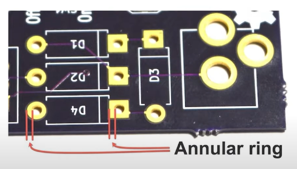
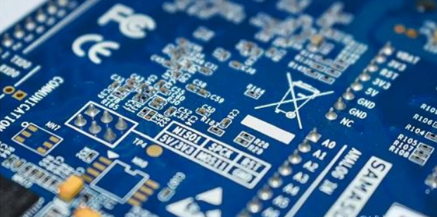
Annular rings in PCBs (printed circuit boards) are the key element that have a major function and provide the PCB design with a trustworthy and functional operation. It deals too much copper, with the additional copper pad area surrounding a plated through-hole on the board. This additional copper land serves several important purposes:
- Component Attachment: Steel rings become a good connection point for electronic components, consisting of resistors, capacitors and integrated circuits, which are soldered on the surface of the PCB. Here the lead components are soldered to the rings which in turn establish electrical bond between the components and conductive traces on the boards.
- Mechanical Support: Besides that, annular rings provide the mechanical support for PCB assembly in addition to its function. They make sure that the component leads stay in place and that they do not come loose because of mechanical stress, vibrations, or if they expand as a result of heat.
- Electrical Connectivity: Represents an efficient technology which provides reliable electrical connection between the component lead and the conductive PCB trace. This relationship is critical to the operation of the circuit, since electrical signals are easily sent to various parts of the PCB because of this connection.
- Signal Integrity: The integrity of the signal paths is the key thing as it keeps the signal clean and enables the proper circuit work. Ideal size helps keep the low impedance and prevent the signal loss which becomes severe in the high frequency applications.
- Manufacturing Considerations: An important dimension that affects the plating quality in PCBs is the size of hole diameters where the drilling accuracy depends on this factor. The board design must be done with the appropriate dimensions in mind in order for production and assembly to be successful.
Generally, annular rings form a core part of PBCs, both in terms of electrical functionality and mechanical stability. Being well adjusted and correctly sized of annular ring plays crucial for the board’s reliability, performance, and manufacturing.
What is the structure of a PCB Annular Ring?
The structural makeup of outer circle of an annular pad on PCB is normally made up of several layers with their unique role to perform to make the printed circuit board work efficiently and reliably. The primary layers that make up the structure of outer ring of a PCB annular pad include:
Copper Layer

The component element of the circuit enters the toroidal structure is its layer. The inner layer is normally laminated with copper foil on the substrate material that makes the PCB. The outer layer provides the conducting tracks for the electrical signals, and serves as the base for soldering components on board.
Substrate Material
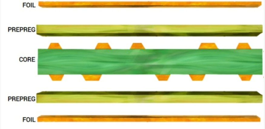
There is one layer of the substrate that is always a non-conductive material usually fiberglass-reinforced epoxy resin (FR-4) which is encircling the ayer. The substrate functions both as mechanical support as well as insulation in between the conductive traces to the copper plated PCB.
Plating
In plated-through hole (PTH) technology, the annular pad will extend into the plated hole to create a solid conductive path from one side to another PCB board interconnection. This kind drilling process of plating through holes in fact is providing electrical interconnectivity amongst layers of the PCB besides helping in strengthening the mechanical tightness of plated holes.
Solder Mask
A solder mask layer is applied over the entire surface board that covers the copper traces leaving the regions intended for soldering exposed. Solder mask not only insures solder bridges between adjacent pads are avoided but also copper traces on solder pad are oxidation and environmental resistant protected.
Silkscreen
On an optional basis, a silkscreen layer can be included with its markings, identifiers and other information for convenient assembly and failure analysis. The silkscreen is the topmost layer, laid on top of the inner layer, the solder mask one.
The structure and inner circle of a PCB annular ring is built to create a stable and reliable junction point for electronic components, maintaining the required electrical conductivity, mechanical strength and shield against environmental detriments. Correct design and manufacture of the circular annular ring pcb and structure are fundamentally vital for the functioning and durability of the PCB.
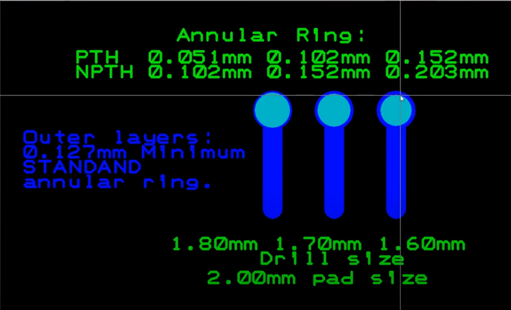
What Is the Minimum Annular Ring in PCB?
The the minimum width of annular ring per copper plate is determined by the manufacturing resolution of the PCB fabrication process, such as precision of the drill equipment, accurate etching of copper features, and specifications set on them. The minimum annular ring width per copper trace for most PCB fabrication processes is around 0.1mm to 0.15mm. It is 4 to 6 mils in the English measurement.
The most important thing is to always follow the minimum pad diameter to help you get good solder of components and solid electrical connections. Any deviations from the specified solder process may cause solder fractures, poor electrical connectivity, and other related problems, which may negatively impact the performance and reliability of the PCB assembly. Consequently, designers should always keep involving PCB manufacturers as well as adhering to industry guidelines while deciding on the minimum annular ring for their designs.
Why Annular Ring Size Matter?
The border width (annular ring) on the printed circuit board (PCB) is important in that it has a direct effect on reliability of soldering, electrical connectivity, mechanical stability, producibility, and design aspects. Correct pad size is used for strong solder joints, ensures consistent electrical connections and provides mechanical support for components and is also contributes for production processes and design requirements. Incorrect PCB annular rings size may result in providing reasons for most of the problems like soldering issues, manufacturing difficulties, poor electrical conductivity, mechanical issues, and design constraints which eventually affect the functionality and reliability of the PCB assemblies. Consequently, choosing the proper annular ring size will bring performance and dependability in the correct application of PCB.
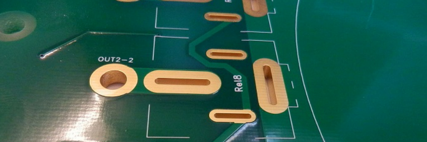
What is the role of a copper pad in Annular Rings?
Copper pad in annular rings is a vital link which ensures a secure and trustworthy place where electronic components gets laid on their respective printed circuit boards (PCB). To wrap it up, the soldering is one of the most fundamental processes for component assembly onto the outer ring surrounding the PCB.
The copper pad provides a high mechanical robustness and the component lead is placed on the pad and therefore the component is prevented from becoming loose or detached during mechanical, mechanical or thermal stress, mechanical or thermal stress, or environmental impact via that pad. Also, the copper pad could do the job of electrical connectivity very well by offering a pathway to pass the signals across the PCB connect traces and the component too.
Considering annular ring dimension especially, the diameter of copper pad diameter encloses the drilled hole as padded-shaped entity. On the other hand, larger pad in the parallel configuration widens a soldering zone, improving a chance to obtain a strong solder joint and making the electrical connectivity a sufficient one. The copper pad size and contour, including the perfect width of annular pad, play a key role in determining the good and versatile PCB mounting performance.
What is Teardrop Annular Ring?
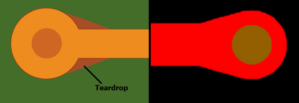
The teardrop annular ring is fitting within the cross-linked circuit boards (PCBs) indicating the pad or trace contract to the outer of holes drilled PTH with a teardrop-like shape. This taper is not normally seen during the “green” state of machining process, and only appears at the junction between the drilled hole and the trace or pad creating a teardrop-like extension just off center of the finished hole.
The teardrop annular ring design is developed for better quality in finish, to improve the well-being and strength of the link between the vague or teardrop pad and finished hole or through-hole. It decreases the possibility of vertical phenomena like raised pads or broken paths which mightlift stress. Namely, it allows stress to be distributed evenly around the diameter of the hole or through-hole diameter. This parameter is crucial in the applications with high mechanical stress or environmentally unstable conditions in which the process could be interrupted by variety of mechanical or thermal stress factors such as cycling or vibration.
What are the common issues of Annular Rings?
The defects related to annular rings in printed circduit boards, among other issues, can affect the functional, reliability of the PCB assembly, and manufacturing process of the PCB components. Here are some of these issues, including bolded feature snippets:
- Insufficient Annular Ring Size: A ring that is oversized for the annulus can cause problems both at the initial joining stage and during the welding process. The lack of space around the diameter of the hole drilled may result in poor soldering and the inability to establish a case between the components and the PCB, which causes intermittent or circuit malfunctioning.
- Annular Ring Breakage: The observing of considered mechanical stress, combination of various through holes, and the drills situation are among causes of annular rings breakage. This issue in addition to weakening the structural integrity of PCB may result in detachment of modules or electrical disconnection which eventually leads to a circuit that is not reliable to use.
- Annular Ring Cracks: Lack of mechanical properties such as shrinkage, stress, or porosity may lead to annular ring cracking while making these rings or during inter-pad assembly stages. An illustration of the weak points which may cause the failure of the zero annular ring and these wires as a result of the cracks include being intermittent or permanent circuit damage.
- Plating Defects: Annular ring faults are of the most dangerous types of defects in plated-through hole technology which depends on the quality of plating in PTHs. Plating gaps or discontinuity in the plating process can cause poor conductivity of the palladium layer (outer layer) followed by the noticeable increase in resistance or open circuits.
- Annular Ring Over-Etching: During the milling process silmlie during the PCB production, an excessive milling may result in a reduction of the annular ring width. The integrity of the annular ring can come into question and the structure can loose its mechanical robustness that may cause incompatibility or mechanic troubles.
- Design Limitations: In certain situations design specifications or implementing restrictions of PCB can impose an annular ring dimension limit. These constraints can be the cause for the clumsiness as well as unreliability of the resultant PCB assembly. Thus, PCB designers are recommended to carefully consider these limitations during the initial stage in order to limit the issues.
Solving these frequent problems means that designers should take into account these issues, adhere to the tolerance limits and perform close inspection during manufacturing and assembly in order to ensure the quality of PCB. The recurrence of annular rings defect results in the failure of printed circuit boards. Thus, by detecting and the mitigation of possible defects relating to annular ring, engineers and PCB manufacturer achieve the reliability structural integrity and functionality of the electronic designed devices.
What are the IPC Guidelines for the PCB Minimum Annular Ring?
The IPC (Association Connecting Electronics Industries) has set standards and guidelines for several aspects in PCB (Print Circuit Board) and PCB (Print Casting Board) design and production, including the required minimum pad diameter. Here are the IPC guidelines for the PCB minimum pad breakout and annular ring, including bolded feature snippets:
Similar to IPC standard, the annular ring size min diameter is usually prescribed based on the ended of drilled and finished hole holes diameter. The distance of the annular ring drilled and finished hole is determined as the through-holes radius minus the copper-pad-surrounding’s radius.
According to the of PCB design IPC-2221, at least one annular ring around hole diameter of 0,1 mm (about 4 mils) should be mandatory for high-quality PCB manufacture everywhere. On the other hand, a specific technical specification or enabling feature might call for the use of another annular size or a larger annular rings or various ring geometries to achieve the desired level of reliability and manufacturability.
Moreover, IPC-A-600, an Acceptability of Printed Boards standard, clearly defines the criteria for creating the quality of printed circuit boards and specifies the annular ring dimensions, as well. It sets the acceptable tolerances and quality criteria for annular ring dimension to have compatibility with the existing industrial protocols and particular customers requirements.
Conclusion
Finally, annular rings manifest the key aspects of board performance allowing to guarantee the reliability, functionality, and manufacture of electronic systems. Rings formed by the laser ablation process provide solid connection points for soldering of electronic components, a vital element of electrical connectivity between components and PCB traces, and an imperative support structure for the whole assembly. Sticking industry standards and norms towards annular ring measures will allow to guarantee solder joint efficiency, mechanical stability and electrical consistency. Sound engineering process of the annular rings with its effective implementation is the key to the elaboration of board assemblies with diverse uses in the production of electronic devices.


